鑫景福致力于滿足“快速服務(wù),零缺陷,輔助研發(fā)”PCBA訂購(gòu)單需求。


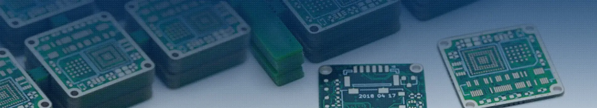
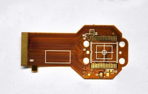
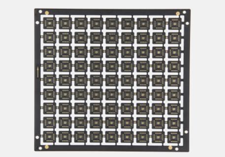
PCB制造
What is PCB soldering? circuit board soldering is the process of soldering components to PCB printed circuit board (bare board). PCB, PCB, PCB welding technology In recent years, the process development of electronIC industry, we can notice a very obvious trend is reflow soldering technology. In principle, traditional inserts can also be reflowed, which is commonly referred to as through-hole reflow soldering. Its advantage is that it is possible to complete all welding points at the same time, so that the production cost is minimized. However, the application of reflow soldering is limited by the temperature sensing element, and people turn their attention to selective soldering, no matter for the plug-in parts or SMDs.

In most applications, selective welding can be used after reflow welding. This will be an economical and effective method of welding the remaining inserts and will be fully compatible with future lead-free welding.
What is PCB welding? Describe the process of PCB welding in detail
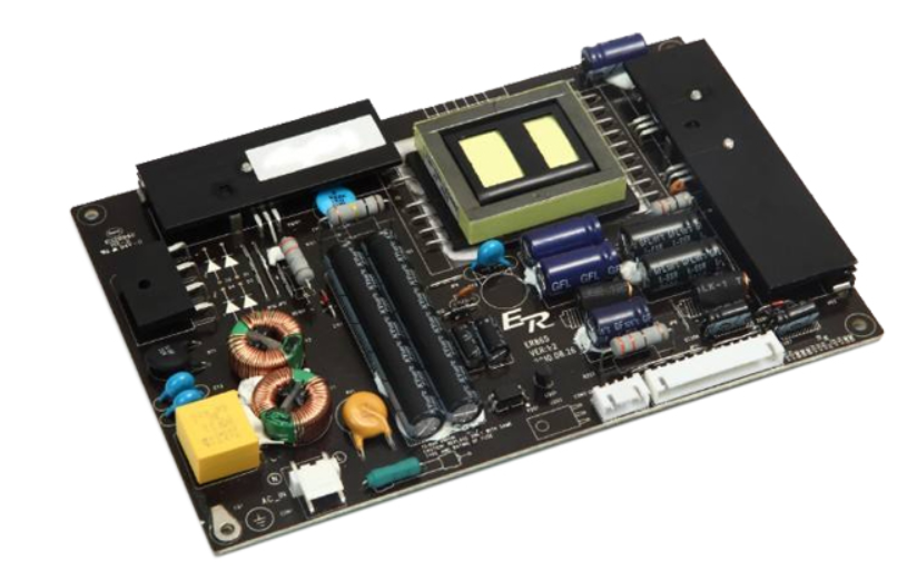
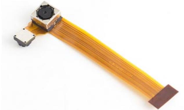
PCB welding is divided into straight plug-in welding and SMD welding
There are generally three types of straight plug-in welding: electric iron welding, immersion welding and wave soldering. Manual electric iron welding is generally used for template and SMAll batch, immersion welding is generally used for small batch, and wave soldering is generally used for large batch.
Patch welding generally includes electric iron welding and reflow welding. Template and SIMple plates generally adopt electric iron welding, while complex plates and large batches generally adopt reflow welding.
Welding process flow of circuit board
1. Preheating
First, the solvent used to achieve the required viscosity and screen printing performance starts to evaporate, and the temperature must rise slowly (about 5 ° C per second) to limit boiling and splashing and prevent the formation of small tin beads. In addition, some elements are sensitive to internal stress, and if the external temperature of the element rises too fast, it will cause fracture.
When the flux (paste) is active and the chEMIcal cleaning action starts, the same cleaning action will occur for both water-soluble flux (paste) and non cleaning flux (paste), but the temperature is slightly different. Remove metal oxides and some contaminants from the metal and solder particles to be bonded. Good metallurgical solder joints require a "clean" surface. When the temperature continues to rise, the solder particles first melt separately, and begin to liquefy and absorb tin on the surface. This covers all possible surfaces and starts to form solder joints.
2. Backflow
This stage is the most important. When all the individual solder particles are melted, they are combined to form liquid tin. At this time, the surface tension starts to form the surface of the solder pin. If the gap between the component pin and the PCB pad exceeds 4mil (1 mil=one thousandth of an inch), it is most likely that the surface tension separates the pin and the pad, causing an open circuit of the solder point.
3. Cooling
In the cooling stage, if the cooling is fast, the tin point strength will be slightly higher, but not too fast, otherwise it will cause the temperature stress inside the element.
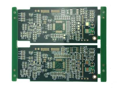
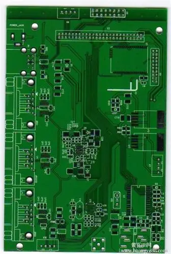
4. PCBA inspection
One is manual welding. First, tin the bonding pad with an electric soldering iron, then clamp one end of the chip element with tweezers, fix the other end of the element on the corresponding bonding pad of the device with a soldering iron, remove the tweezers after the soldering tin is slightly cooLED, and then weld the other end of the element with a soldering iron.
The second is machine welding. The method is to make a blank stencil, print solder paste on the circuit board, place the welded chip components manually or by machine mounting, and finally weld the chip components through a high-temperature welding furnace.
What equipment is required for circuit board welding
Soldering patch components generally require a soldering gun, clip, magnifying glass, solder paste, rosin oil or paste, etc
How to weld SMD components_ What equipment is required for circuit board welding
Weld the other side after the patch is fixed! When soldering the IC, first fix one leg of the chip IC on the PCB, and then find a thin copper wire and rosin like brushed apple to put on the IC leg! Use copper wire to absorb tin and then use alcohol to clean (use cotton swab). You will find that the rosin will melt and disappear! Do some finishing work.
This article is about what is PCB welding, and introduces the process of PCB welding in detail

抖音二維碼

Q Q二維碼

微信二維碼
點(diǎn)擊
然后
聯(lián)系
然后
聯(lián)系
電話熱線
13410863085Q Q

微信

- 郵箱