鑫景福致力于滿足“快速服務,零缺陷,輔助研發(fā)”PCBA訂購單需求。


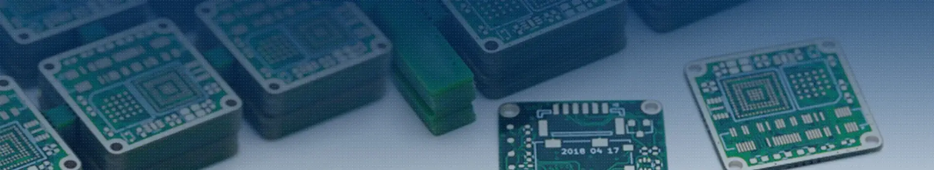
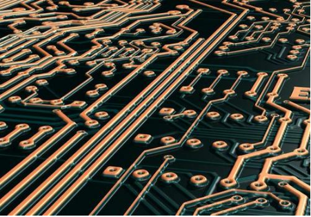
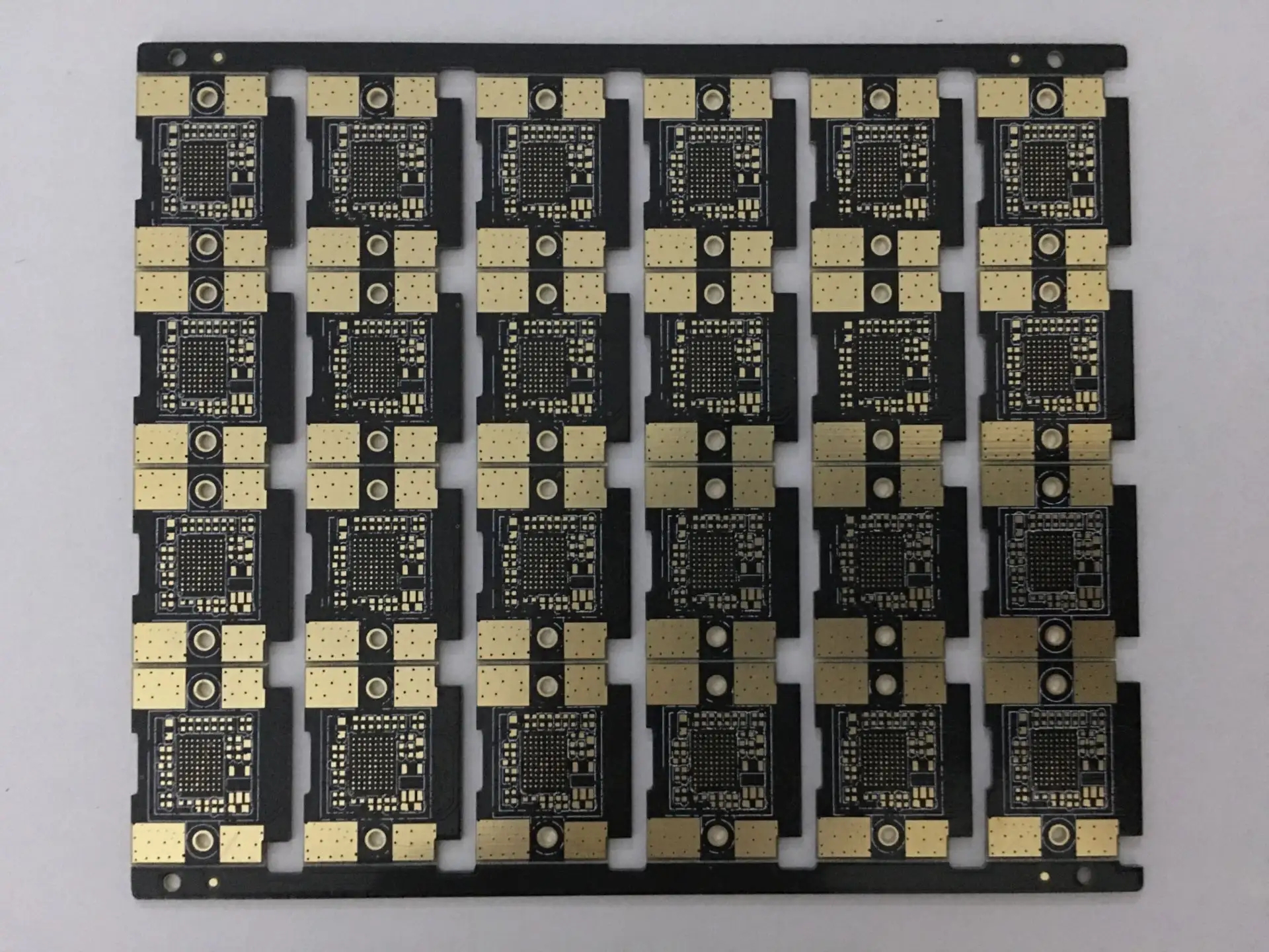
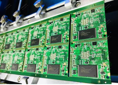
PCB制造
Briefly, I will tell you the layers and functions used in general PCB copying. (The following colors are default and can be modified by yourself)
The line drawn by the TopLayer (top layer) is red, whICh is the upper layer of the general double-sided panel, and the single panel can not use this layer
The line drawn by the Bottom Layer is blue, which is the line layer above the single-sided board.
MidLayer1 This is the first intermediate layer. It seems that there are 30 layers. Generally, PCB designers cannot use it. You don't need to worry about it. It is used when there are multiple panels. It is not displayed in 99SE by default. Not really.
Mechanical Layers (magenta) are used to MARK the size. The board description is ignored during PCB copying, that is, the board is invisible when it is made. The meaning of SIMple punctuation notes.
Top Overlay (yellow) is the character on the front of the board, which corresponds to the TopLayer single panel. Bottom Overlay (brown) corresponds to the BottomLayer, which corresponds to the character on the back of the board. The two layers of characters are used when double panels are used.
KeepOutLayer (the same as the mechanical layer) is simply the frame and appearance of the board.
Multi layer (silver) All wiring layers include single and double side plug-in pads, and the spline lines are drawn on all layers.
1. TopLayer (top layer) The top wiring layer is used to draw the electrical connection lines between components.
2. BottomLayer (bottom layer) The bottom wiring layer acts on the top wiring layer.
3. MidLayer1 (middle layer 1) is used to draw electrical connection lines on this layer when making multilayer boards, but the cost of Multilayer boards is relatively high.
4. Mechanical Layers can be used to draw the shape of PCB and the parts to be hollowed, or to annotate PCB dimensions. It can be used to draw the shape of PCB and the parts to be hollowed. Note that PCB shapes, hollowed parts and PCB annotation dimensions do not use the same mechanical layer. For example, mechanical layer 1 is used to Draw PCB shapes and hollows, and mechanical layer 13 is used to annotate dimensions, After separation, the technicians of the PCB manufacturer will analyze whether it is necessary to make this layer according to its contents.
5. Top Overlay (yellow) is the character on the front of the board, which corresponds to the TopLayer single panel. Bottom Overlay (brown) corresponds to the BottomLayer, which corresponds to the character on the back of the board. The above two layers of characters are used when double panels are used.
6. KeepOutLayer is used to draw the forbidden wiring area. If there is no mechanical layer in the PCB, the PCB manufacturer will use this layer as the PCB shape. For example, in the case of both KEEPOUT LAYER layer and mechanical layer, the mechanical layer is used as the PCB shape by default, but the PCB manufacturer's technicians will distinguish it by themselves, but if they can't distinguish it, they will use the mechanical layer as the shape layer by default.
7. All wiring layers of the Multi layer (silver) include single and double sided plug-in pads. The lines are drawn on all layers.
1、 Signal Layers
Protel98 and Protel99 provide 16 signal layers: Top, Bottom and Mid1-Mid14.
The signal layer is the wiring layer used to complete the copper foil routing of the printed circuit board. When designing double-sided boards, only the top layer and bottom layer are generally used. When the number of printed circuit boards exceeds 4, Mid (intermediate wiring layer) is required.
2、 Internal Planes
Protel98 and Protel99 provide Plane1-Plane4 (4 internal power supplies/ground planes). The internal power/ground plane is mainly used for more than 4 layers of printed circuit boards as the special wiring layer for power and grounding, and the double-sided board does not need to be used.
3、 Mechanical Layers
The mechanical layer is generally used to draw the border (boundary) of the printed circuit board, and usually only one mechanical layer is used. There are Mech1-Mech4 (4 mechanical layers).
4、 Drkll Layers
There are two layers: "Drill Drawing" and "Drill Guide". Used to draw the hole diameter and the location of the hole.
5、 Solder Mask
There are 2 layers: Top and Bottom. The protective area around the pad and via on the printed circuit board when drawn on the solder mask.
6、 Paste Mask
There are 2 layers: Top and Bottom. The solder paste protective layer is mainly used for printed circuit boards with surface mounted components. This layer is required by the installation process of surface mounted components, and it is not required when there is no surface mounted components.
7、 Silkscreen
There are 2 layers: Top and Bottom. The silk screen layer is mainly used to draw text descriptions and graphic descriptions, such as outline, label and parameters of PCB components.
8、 Other
There are 8 layers in total: "Keep Out", "Multi Layer", "Connect", "DRC Error", 2 "Visible Grid", "Pad Holes" and "Via Holes". Some of these layers are used by the system itself. For example, the Visible Grid is designed to facilitate designers' positioning during drawing. The Keep Put layer is used for automatic routing, and manual routing is unnecessary.
For manual drawing of double-sided printed circuit boards, the top layers, bottom layers and top silk screen are used most frequently. Each layer can choose its own color. Generally, red is used for the top layer, blue is used for the bottom layer, green or white is used for text and symbols, and yellow is used for pads and vias.
Top layer and bottom layer: they are the top layer and bottom layer respectively, that is, the upper layer and the lower layer of the circuit board surface. Usually, signal lines are arranged on the top, such as double-layer boards. For multilayer boards, signal layer wiring can also be added in the middle.
Mechanical layer: defines the appearance of the entire PCB, that is, the overall structure of the PCB.
Keepoutlayer keepoutlayer: defines the boundary on the copper side of the cloth electrical characteristics. That is to say, after the forbidden wiring layer is defined first, the wires with electrical characteristics laid in the subsequent wiring process cannot exceed the boundary of the forbidden wiring layer.
Topoverlay top silk screen layer
Bottom overlay bottom silk screen layer: defines the top and bottom silk screen characters, which are the component numbers and some characters commonly seen on PCB boards.
Toppaste top pad layer
Bottompaste bottom bonding pad layer: refers to the copper and platinum exposed outside.
Topholder top layer
Bottomsolder bottom layer: opposite to toppaste and bottompaste, it is the layer to be covered with green oil.
Drillguide via guide layer
Drilldrawing through hole drilling layer
Multiplayer: refers to all layers of PCB.
1. TopLayer component layer, BottomLayer wiring and plug-in component welding layer, MidLayerx intermediate layer, these layers are used to draw wire or copper coating (of course, there is also the pad PAD of SMT chip devices of TopLayer and BottomLayer);
2. Top Solder, Bottom Solder, Top Paste and Bottom Paste are related to the device PAD passing through more than two layers; Generally, the holes left in the Paste layer will be SMAller than the pads (Paste surface means the solder paste layer, which means that it can be used to make the steel MESh for printing solder paste. This layer only needs to expose all pads that need to be pasted and welded, and the holes may be smaller than the actual pads); Then, brush green oil (solder mask) on the pcb board. This is the Solder layer. The Solder layer should expose the PAD. This is the small circle or square circle we see when only the Solder layer is displayed, Generally, it is larger than the PCB pad (Solder surface means a solder mask layer, which is used to coat solder mask materials such as green oil, so as to prevent solder from contaminating areas that do not need to be welded. This layer will expose all pads that need to be welded, and the hole will be larger than the actual pad); These layers are generally yellow (copper) or white (tin);
3. Top Overlay, Bottom Overlay, silk screen layer, characters or resistance capacitance symbols or device borders on PCB surface, generally white;
4. Keep out, draw a border to determine the electrical boundary;
5. The Mechanical layer, the real physical boundary, and the positioning hole are made according to the size of the Mechanical layer, but the Pcb factory engineers generally do not understand this. Therefore, it is better to delete the keepout layer layer before sending it to the PCB factory;
6. Multi Layer, which runs through all layers, such as vias (VIAs of the bottom layer or top layer also have Solder and Paste).

抖音二維碼

Q Q二維碼

微信二維碼
點擊
然后
聯(lián)系
然后
聯(lián)系
電話熱線
13410863085Q Q

微信

- 郵箱