
ElectronIC Engineering Manufacturing: How to Reduce "PCB ground Spring Effect"
Circuit board manufacturing, circuit board design and PCBA processing manufacturers explain electronic engineering manufacturing: how to reduce the "PCB ground spring effect"
1. What is a ground bullet
1.1. Concept of ground bomb
Ground spring, ringing, crosstalk and signal reflection are always the key objects in signal integrity analysis. The beginner has a look: How profound! In fact, the feeling is profound because you hear the word "earth bounce" all over the sky, but you can't find the "real principle of earth bounce" everywhere. If you carefully read the author's chapter "The Origin of Noise", in fact, you already know the earth bomb! Earth bombs are ground noise!
1.2 Why is it calLED Earth Bullet
Since it is ground noise, why is it called "ground bounce"? Why is it that since it is the same thing, it has changed its name, which makes me puzzled?
At low frequencies, the ground noise is mainly due to the "resistance" of the conductor constituting the ground wire, and the potential difference fluctuation caused by the current of the circuit system flowing through the ground wire.
At high frequency, the ground noise is mainly due to the "inductance" of the conductor constituting the ground wire. When the current of the circuit system passes through this "inductance" with rapid changes, stronger voltage disturbances will be excited at both ends of the "inductance", which is vividly called "ground bounce".
Earth bomb, generally for IC. Because the "circuit ground" inside the chip and the "ground pin" of the chip are actually connected by a very thin gold wire, the gold wire has a large inductance, which may cause a strong "voltage difference fluctuation" between the ground of the circuit inside the chip and the ground of the real PCB - a strong ground bounce phenomenon!
Unlike PCB board, this ground spring can be weakened by increasing decoupling capacitance. Suppose you have a B PCB and a A motherboard; B PCB board is inserted on the main board for use. Then suppose that the ground wire connection points of A and B are not large enough. When there is high-speed signal communication between A and B, the "ground plane" on board B and the "ground plane" on board A will have a large "ground voltage difference fluctuation". This is also a kind of "ground spring effect" on PCB.
The earth bomb is actually the alias of "ground noise". Just understand! I guess you don't have to look down.
2. Formation Mechanism and Harm of Ground Bullet
I didn't want to write about the mechanism of the earth bomb, but the feeling is the same as the "origin of noise". However, after thinking about it, I felt that such a classic question was not afraid to mention it more, so I wrote it down again.

2.1 Formation mechanism of earth bomb
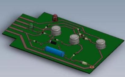
The red box represents a digital circuit. It has been described in the chapter "Origin of Noise" that when S5 is constantly switching left and right in the following figure, due to the existence of R14 resistance between E and A on the ground wire, point E will generate potential difference relative to point A. In high frequency state, the main cause of potential difference between E and A is no longer "resistance between E and A", but "inductance between E and A".
The ground noise of "E point ground" relative to "A point ground" is the ground bounce phenomenon when the circuit system is working.
2.2 Hazards of ground bullets
According to the chapter "Origin of Noise", ground noise (ground bounce) is equivalent to the external "input ground noise" in a circuit with "ideal ground". So, if there is 1MHz ground noise at point E, what harm will it do?
2.2.1 According to the analysis of "the harm of the ground loop" in the previous chapter, if the digital module in the box in the above figure has 20 signal lines, the ground noise will directly reflect on the 20 signal lines, thus affecting the waveform quality of these signals and radiating outward through the 20 signal lines.
2.2.2 Ground spring makes ground wire radiate
You may ask: Does the ground wire also generate radiation? You may have read some books about PCB wiring that describe that incorrect flooring will produce "ground wire radiation", which will aggravate interference—— But you don't understand its principle, and even doubt whether the book author has made mistakes! Let me tell you, there may be radiation in the ground wire!
In this example, point E has a 1MHz ground noise relative to point A, so the whole blue ground wire has a 1MHz noise relative to point A. Because the ground wire is pulled on the edge of the PCB board for a long time, this wire is like a transmitting antenna (long shape, with 1MHz "signal to be transmitted" on it), and it continuously transmits "ground noise".
3. How to reduce "PCB ground spring effect"
3.1 Add appropriate decoupling capacitance
In fact, in order to reduce the interference of 1MHz on the whole circuit, we add a decoupling capacitor C7 between points D and E.
The equivalent circuit analysis is as follows (note that the equivalent circuit is not very accurate, but the general principle can be described. The model should be considered and analyzed by the reader after technical advancement): Since the capacitive reactance of C is Zc=1/(2 π fc), the equivalent effect for 1MHz noise of power supply and ground is R34 in Figure 3.1-2.
Since the impedance of R34 is far less than (R32+R33+R35), and the "noise signal source" has a considerable "internal resistance", two effects will be produced: 1. Most of the energy of the "noise signal source" will pass through R34 - so most of the noise energy will disappear through the "(1)" loop in the figure to form a SMAll circulation path. Although this energy is strong, it will not interfere with circuits other than "(1)"; Only a small part of the energy "escapes" from the "(1)" loop and interferes with other circuits with weak energy. 2. The 1MHz square wave interference of the "noise signal source" will no longer exist and will be filtered by C7 into a waveform SIMilar to the sine wave with smooth changes.
The advantages are: 1. The loop area is reduced, the high-frequency radiation energy is reduced, and the EMC interference will be greatly reduced; 2. Square wave interference becoMES sine wave interference, and its higher harmonic component will be greatly reduced, so its interference ability will also be greatly reduced! Ha ha, it's so harmonious! Now, do you understand why a power decoupling capacitor should be connected to the power supply terminal of a digital chip? Why do many books about PCB wiring appear "to add power decoupling capacitor"?
3.2 Use thick and short "ground wire"
The ground noise is caused by the resistance and inductance of the ground wire. Therefore, we should reduce the "resistance and inductance" of the ground wire. When the ground wire increases and its length decreases, its resistance and inductance will decrease, thus successfully reducing the ground noise. In this way, the ground bullets will be greatly reduced!
Therefore, when PCB layout wiring can use thick ground wires, do not use thin ground wires; If you can use a short ground wire, don't use a long ground wire.
Note: Do not blindly lengthen N times the power cord in order to shorten a little ground wire. Both power and ground are very important, and specific analysis must be made for specific problems. Therefore, it is still the same sentence that the reader should pay attention to the principle rather than the specific "method of shortening the ground wire".
4. Focus
1. Earth bomb is ground noise
2. The earth bullet radiates the ground wire
3. Adding an appropriate decoupling capacitor can reduce the ground spring effect between modules
4. Focus on principles rather than specific practices
The manufacturers of circuit board manufacturing, circuit board design and PCBA will explain to you how to reduce the "PCB ground spring effect" in electronic engineering manufacturing.
然后
聯系
電話熱線
13410863085Q Q

微信

- 郵箱


