鑫景福致力于滿足“快速服務,零缺陷,輔助研發”PCBA訂購單需求。


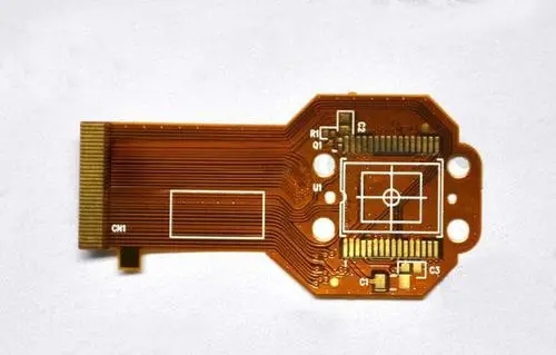
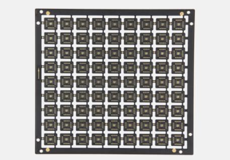
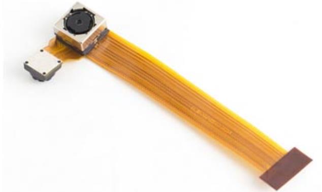
PCB制造
Effective solutions to PCB thICk copper plate warping that must be known
1、 Why PCB thick copper plate is required to be very flat
In the automatic insertion line, if the printed circuit board is not flat, it will cause inaccurate positioning, and components cannot be inserted into the holes of the board and surface mount pads, or even damage the automatic insertion machine. The boards with components are bent after welding, and it is difficult to cut the component legs in order. In this case, the PCB board cannot be instalLED on the chassis or the socket inside the machine, so the assembly plant is also very worried about the board warping. At present, the printed circuit board has entered the era of surface mounting and chip mounting, and the assembly plant must have more strict requirements on board warping.
2、 Standard and test method for warpage
According to (Qualification and Performance Specification for Rigid Printed Boards), the maximum allowable warpage and twist for surface mounted printed boards is 0.75%, and 1.5% for other kinds of boards. At present, the allowable warpage of each electronic assembly plant is 0.70-0.75%, regardless of double-sided circuit boards or multilayer circuit boards, PCB thick copper boards, 1.6mm thick, and many SMT and BGA boards, which are required to be 0.5%. Some electronic factories are encouraging to raise the warpage standard to 0.3%. Put the printed board on the verified platform, insert the test pin at the place with the maximum warpage, and calculate the warpage of the printed board by dividing the diameter of the test pin by the length of the curved edge of the printed board.
3、 Anti warping of PCB thick copper plate during manufacturing
1. Engineering design:
Precautions for PCB design:
A. The arrangement of interlayer prepreg should be symmetrical, such as six layers of pcb board. The thickness between 1~2 and 5~6 layers should be consistent with the number of prepreg sheets, otherwise it is easy to warp after lamination.
B. Multilayer circuit board core board and prepreg shall be from the same supplier.
C. The area of the outer layer A and B lines should be as close as possible. If the A side is large copper and the B side only runs a few wires, this kind of printed board is easy to warp after etching. If the difference between the line areas on both sides is too large, some independent grids can be added on the thin side for balance.
2. Drying plate before blanking:
The purpose of baking the PCB thick copper plate before blanking (150 ° C, 8 ± 2 hours) is to remove the moisture in the plate, and at the same time to completely solidify the resin in the plate, further eliminating the residual stress in the plate, which is helpful to prevent the plate from warping. At present, many double-sided and multi-layer PCB boards still adhere to the process of drying before or after blanking. However, there are some exceptions to this rule. At present, the drying time of PCB plants is also inconsistent, ranging from 4 to 10 hours. It is recommended to decide according to the grade of PCB produced and the customer's requirements for warpage. The two methods are both feasible, and it is recommended to bake the board after shearing. The inner plate shall also be baked.
3. Longitudinal and latitudinal directions of prepreg:
After laminating, the shrinkage of the prepreg in the warp and weft direction is different. The warp and weft directions must be distinguished when blanking and laminating. Otherwise, it is easy to cause warping of the finished board after lamination, and it is difficult to correct even if the pressure is applied to bake the board. Many reasons for the warping of multilayer boards are due to the disorderly overlapping of the warp and weft directions of the prepreg during lamination.
How to distinguish longitude and latitude? The roll up direction of the rolled prepreg is the warp direction, while the width direction is the weft direction; For copper foil, the long side is in the weft direction and the short side is in the warp direction. If you are not sure, you can check with the manufacturer or supplier.
4. Stress relief of PCB thick copper plate after lamination:
After hot pressing and cold pressing, take out the multilayer PCB board, cut or mill off the burrs, and then place it flat in the oven at 150 ℃ for drying for 4 hours to gradually release the stress in the board and completely cure the resin. This step cannot be omitted.
5. The sheet needs to be straightened during electroplating:
When the 0.4~0.6mm ultra-thin multilayer board is used for plate surface electroplating and graphic electroplating, special clamping rollers shall be made. After the thin plate is clamped on the fly bar on the automatic electroplating line, a round bar shall be used to string the clamping rollers on the whole fly bar, so as to straighten all the plates on the roller, so that the plates after electroplating will not be deformed. Without this measure, the thin plate will be bent and difficult to repair after electroplating 20 to 30 micrometers of copper layer.
6. Cooling of plates after hot air leveling:
When PCB thick copper plate is leveled by hot air, it will be impacted by the high temperature of solder bath (about 250 ℃). After being taken out, it should be placed on flat marble or steel plate for natural cooling, and then sent to the post-processing machine for cleaning. This is good for warping prevention of boards. Some factories, in order to enhance the brightness of the lead tin surface, put the boards into cold water immediately after hot air leveling, and take them out for post-treatment after a few seconds. This impact of one hot and one cold may cause warping, delamination or blistering of some models of boards. In addition, air floating bed can be installed on the equipment for cooling.
7. Treatment of warped boards:
In a well managed PCB factory, 100% flatness inspection will be carried out for printed boards during final inspection. All unqualified boards will be picked out and put into an oven, dried at 150 ℃ and under heavy pressure for 3-6 hours, and naturally cooled under heavy pressure. Then, take out the boards by pressure relief and check the flatness. This can save some boards. Some boards need to be baked for two or three tiMES before leveling. If the anti warping process measures mentioned above are not implemented, the baking and pressing of some boards are useless and can only be scrapped.

抖音二維碼

Q Q二維碼

微信二維碼
點擊
然后
聯系
然后
聯系
電話熱線
13410863085Q Q

微信

- 郵箱