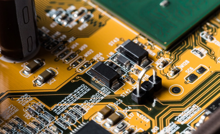

Return path of PCB
Know that the PCB will use the plane closest to the signal path Then 2 is based on these two specifIC conditions
1) When we say four layers, the first, second and third layers are signal layers, and the continuous ground plane is on the fourth layer. For all 3-layer signals, the return current path will be in the fourth plane because there is no other plane.
2) For the second case, the 4-layer superposition is the signal ground plane signal. Suppose there is a signal track on layer 3, but I also inject copper into some VCC tracks in some areas (incomplete) of layer 3. Then, if I draw a signal trace on the fourth layer, the return current will be injected into the grounding plane of the second layer or part of the copper of the third layer, and this trace will pass under the part of the copper casting, not on the part of the next copper casting.
I hope I know.
If you send some photos, it will be clearer. In addition: What is a PCB used for high-speed signals? If not, remember that the return current (actually any current) always follows the path with the least impedance-
For DC and low-frequency filling (<several MHz/>hundreds of ns long switch edge, don't worry about too much RF magic), the ground will be the return path. After entering the VHF range, the return path is usually the path with the least impedance. If your VCC power board has a lot of ceramic decoupling, the return current will flow along the nearest laminar flow (that is, it has good capacitive coupling with the ground or the ground)
Circuit board

This PCB capacitor has an impact on the return current, because the return path is a huge road, and the capacitor is located near the pin I only know one thing about dec Hat They have frequencies Therefore, by connecting some of them in parallel, we obtain low impedance, which provides a more constant voltage level that we want
In this case, since continuous grounding may have the lowest impedance, this will be the return current path of our PCB, because the impedance of partial copper pouring on any layer cannot be lower than that of completely poured grounding layer-
However, how to reach each plane (via) will have a greater impact on the impedance of copper dumping on the plane.
Ceramic decoupling capacitors are very close to short circuiting high frequency signals, which is why they allow the return current to pass between layers at the high end of the frequency range. DC/low frequency may pass through the ground plane, but if there is a close decoupling capacitor, then things with multiple frequencies will want to be as close to the signal track as possible, so that high frequency can be closer to the signal track along the VCC layer, and so on. If nothing operates at a frequency of several megabytes and nothing generates a switch edge lower than 100ns, then I won't worry.
But there is no actual contact. I mean, if we connect a track from the source to the sink, such as from the MCU pin to the i2c sensor pin, then the electromagnetic field will complete this work, and the current will return along the same path, but on a plane. In fact, in my opinion, we have no physical connection with anywhere. I'm confused:)-
It is actually important to summarize all these details, such as impedance ground plane layer stacking at high speed or high frequency. I don't need to worry too much at low frequencies. Mcu sensor and other circuits-
The current will separate all possible paths according to its impedance. The shortest and more conductive path will get more current, not longer and less conductivity. But you can consider the combination of each wire/through-hole/connector/equal resistance and (usually SMAller) capacitance and inductance. Then, you must solve the resulting network to obtain current and voltage values everywhere. Usually this is not important, because there is a wide path, almost all currents are like this, the impedance in the path is very small, and the voltage is almost zero.
Why do you care about reflow? Are you concerned about radiated EMIssions or signal integrity? Or something else? In any case, the fastest edge signal shall always be sent to the position next to the continuous plane If the aircraft has any interruption, please do not send the fast edge signal pcb circuit board when the circuit breaker is disconnected This applies to both stacking options The clock and any signal with fast rising and falling time shall be placed close to GND If you place GND in the inner layer, you can place two trace layers next to GND Considerations
The above is the explanation given by the editor of pcb circuit board company.
If you want to know more about PCBA, you can go to our company's home page to learn about it.
In addition, our company also sells various circuit boards,
High Frequency Circuit Board and SMT chip are waiting for your presence again.
然后
聯系
電話熱線
13410863085Q Q

微信

- 郵箱


