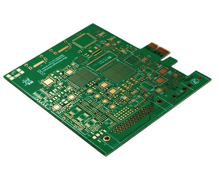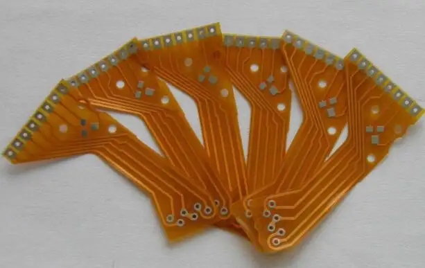

PCB surface technology gold plating, gold precipitation and nICkel palladium
In PCB surface treatment process, we often confuse several treatment processes: gold plating, gold precipitation and nickel palladium. What are the differences between them?
1. Gold plating
The gold plating uses real gold. Even if only a very thin layer is plated, it already accounts for nearly 10% of the cost of the entire circuit board. Gold plating uses gold as the plating layer, one is to facilitate welding, the other is to prevent corrosion; Even the golden fingers of memory modules that have been used for several years are still shining as before.
Advantages: strong conductivity, good oxidation resistance, long service life; The coating is dense and wear-resistant. It is generally used for welding and plugging.
Disadvantages: high cost, poor welding strength.
2. Melting/depositing gold
Nickel leaching (ENIG), also known as nickel leaching gold and nickel precipitation gold, is referred to as nickel leaching gold and gold precipitation. Gold deposition is a chEMIcal method that wraps a thick layer of nickel gold alloy with good electrical properties on the copper surface, and can protect PCB for a long time. The deposition thickness of inner nickel is generally 120~240 μ In (about 3-6 μ m) The deposit thickness of outer layer gold is generally 2-4 μ inch(0.05~0.1 μ m)。 Gold deposition can make PCB achieve good conductivity during long-term use, and it also has the environmental tolerance that other surface treatment processes do not have.
Advantages: 1. The plated PCB surface is very flat and coplanar, which is suitable for the contact surface of keys. 2. The solderability of the gold deposit is excellent. The gold will quickly melt into the molten solder to form metal compounds.
Disadvantages: the process flow is complex, and strict control of process parameters is required to achieve good results. The most troublesome thing is that the PCB surface treated by gold deposition is easy to generate black disk benefits, affecting reliability.

3. Nickel palladium
Compared with nickel gold, nickel palladium (ENEPIG) has an additional layer of palladium between nickel and gold. During the deposition reaction of replacement gold, electroless palladium plating will protect the nickel layer and prevent it from being excessively corroded by the replacement gold; Palladium is fully prepared for gold leaching while preventing corrosion caused by displacement reaction. Nickel deposition thickness is generally 120~240 μ In (about 3-6 μ m) , the thickness of palladium is 4~20 μ In (about 0.1~0.5 μ m); The deposit thickness of gold is generally 1~4 μ in(0.02~0.1 μ m)。
Advantages: It has a wide range of applications, and nickel palladium is relatively precipitated at the same time, which can effectively prevent connection reliability problems caused by black disc defects.
Disadvantages: Although nickel palladium has many advantages, palladium is expensive and a scarce resource. At the same time, as with gold deposition, its process control requirements are strict.
What are the classification and composition of PCB vias?
Via is an important part of PCB, and the cost of drilling usually accounts for 30% to 40% of the cost of PCB manufacturing. In short, each hole on a PCB can be calLED a via. What are the classification and composition of PCB vias?
1、 Classification of vias
From the perspective of function, vias can be divided into two categories: one is used as electrical connection between layers; Second, it is used for fixing or positioning components. In terms of process, vias can be divided into three categories, namely blind holes, buried holes and through holes.
The blind hole is located on the top layer and bottom layer of the circuit board, and has a certain depth. It is used for the connection of the surface line and the inner line. The depth of the hole usually does not exceed a certain ratio (aperture).
The embedded hole is the connection hole in the inner layer of the circuit board, which will not extend to the surface of the circuit board. The above two types of holes are located in the inner layer of the circuit board and are completed by the through hole forming process before lamination.
Through hole refers to the hole through the whole circuit board, which can be used for internal interconnection or as the installation and positioning hole of components. Because through-hole is easier to realize in process and lower in cost, it is used in most PCB proofing.
2、 Composition of vias
From the design point of view, vias are mainly composed of two parts, one is the drilling in the middle, and the other is the pad area around the drilling. The size of these two parts determines the size of the vias. In high-speed and high-density PCB design, designers always hope that the SMAller the vias are, the better, so that more wiring space can be left on the board. However, the reduction of hole size brings about an increase in cost, and the via size is limited by drilling and electroplating technology: the smaller the hole is, the longer it takes to drill, and the easier it is to deviate from the center; And when the depth of the hole exceeds 6 tiMES of the drilling diameter, it is impossible to ensure that the hole wall can be uniformly copper plated.
PCB manufacturing, PCB design and PCBA processing manufacturers will explain the PCB surface technology of gold plating, gold precipitation and nickel palladium.
然后
聯系
電話熱線
13410863085Q Q

微信

- 郵箱


