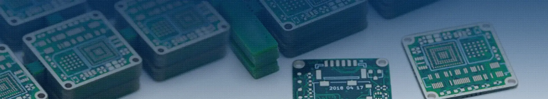
鑫景福致力于滿足“快速服務,零缺陷,輔助研發”PCBA訂購單需求。


PCB制造
What is PCB and what subjects do I need to learn to design PCB?
We discuss the composition of PCB, including some terms, a brief assembly method, and a brief introduction to the PCB design process.
PCB (Printed circuit board) is the most common name, whICh can also be calLED "printed wiring boards" or "printed wiring cards". Before the appearance of PCB, the circuit was composed of point-to-point wiring. The reliability of this method is very low, because with the aging of the circuit, the rupture of the line will lead to the open circuit or short circuit of the line node.
Winding technology is a major progress in circuit technology. This method improves the durability and replaceability of the line by winding SMAll diameter wire on the column of the connection point.
When the electronic industry develops from vacuum tubes and relays to silicon semiconductors and integrated circuits, the size of electronIC components is reduced, and the price is also declining. Electronic products appear more and more frequently in the consumer field, prompting manufacturers to find smaller and more cost-effective solutions. Thus, PCB was born.
Composition
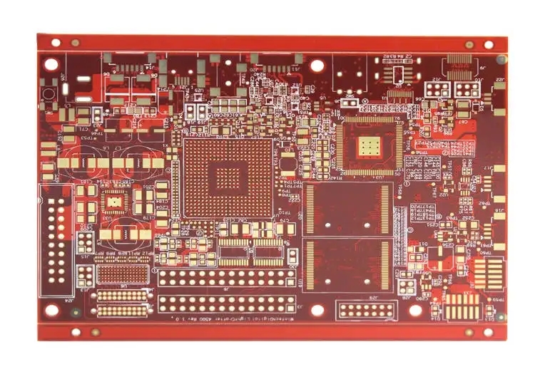
PCB looks like multi-layer cake or thousand layers -- layers of different materials are pressed together by heat and adhesive.
Start from the middle tier.
FR4
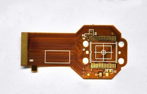
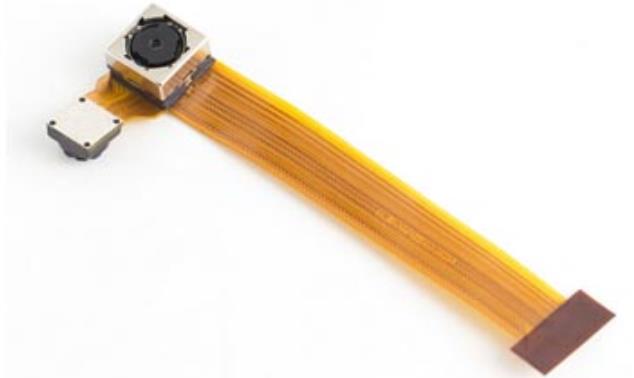
The substrate of PCB is generally glass fiber. In most cases, the glass fiber substrate of PCB generally refers to "FR4". The solid material "FR4" gives PCB hardness and thickness. In addition to FR4, there are flexible circuit boards produced on flexible high-temperature plastics (polyimide or SIMilar).
You may find PCB with different thickness; However, the thickness of most SparkFun products is 1.6mm (0.063 ''). Some products also use other thicknesses, such as LilyPad and Arudino Pro Micro boards, which use a plate thickness of 0.8mm.
Cheap PCB and hole board (see the figure above) are made of materials such as epoxy resin or phenol. They lack the durability of FR4, but they are much cheaper. When you weld something on this board, you will SMEll a lot of strange smell. This type of substrate is often used in low-end consumer goods. Phenolic substances have low thermal decomposition temperature, and too long welding time will cause them to decompose and carbonize, and give off an unpleasant smell.
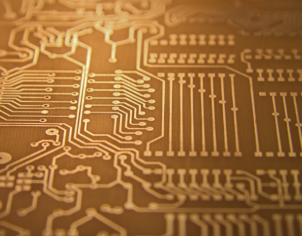
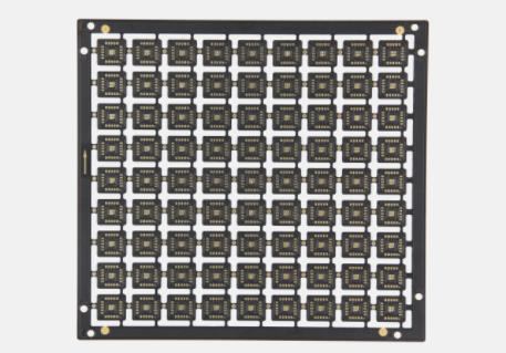
Next, we will introduce the thin copper foil layer, which is pressed onto the substrate by heat and adhesive during production. On the double-sided plate, the copper foil will be pressed to both sides of the substrate. In some low-cost occasions, copper foil may only be pressed on one side of the substrate. When we mention "double-sided board" or "two-layer board", we mean that there are two layers of copper foil on our thousand layers. Of course, in different PCB designs, the number of copper foil layers may be as small as one layer, or more than 16 layers.
There are many kinds of copper layer thickness, and the thickness is measured by weight. Generally, the weight of copper evenly covering one square foot (oz) is used to express the thickness. The copper thickness of most PCBs is 1oz, but some high-power PCBs may use 2oz or 3oz copper thickness. To convert the ounce (oz) per square foot, it is about 35um or 1.4mil thick copper.
Soldermask
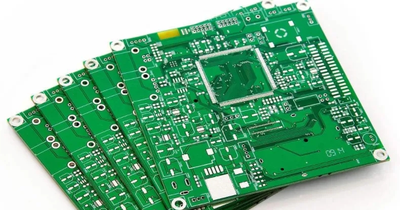
Above the copper layer is a solder mask. This layer makes the PCB look green (or SparkFun red). The solder resistance layer covers the wiring on the copper layer to prevent the wiring on the PCB from contacting with other metals, solders or other conductive objects and causing short circuits. The existence of solder barrier layer enables everyone to weld at the right place and prevents solder bridging.
Soldering resistance covers most of the PCB (including wiring), but the silver hole ring and SMD pad are exposed to facilitate welding.
Generally speaking, resistance welding is green, but almost all colors can be used for resistance welding. Most SparkFun boards are red, but IOIO boards are white and LilyPad boards are purple.
Silkscreen
Above the solder mask is a white silk screen layer. Letters, numbers and symbols are printed on the screen printing layer of PCB, which can facilitate assembly and guide you to better understand the Board Design. We often use the symbol of the screen layer to MARK the function of some pins or LEDs.
The most common color of the screen layer is white. Similarly, the screen layer can be made into almost any color. Black, gray, red and even yellow silk screen layers are not uncommon. However, it is rare to see multiple screen layer colors on a single board.
What subjects do I need to learn to design PCB by myself?
1、 Circuit principle
1. First, understand the PCB design software design process, software installation and unloading, window interface, environmental parameters and document management; Editor and setting project options;
2. Master the basic schematic drawing tools, drawing tools, component position adjustment, and attribute editing; Drawing parameter setting and connecting line;
3. Master the basic operation and tool of component diagram of component library editor; Design of layer schematic diagram
2、 Some Foundations of PCB design
1. Understand the structure of circuit board and the drawings and basic processes in the design of layer circuit board;
2. Master the creation of PCB design files, PCB design environment settings, PCB design manager and PCB design editor;
3. Master the opening, closing and use of toolbars, status bars, command lines and various panels in the editor;
4. Master the use of relevant operation tools for PCB layer and contour definition, and plan the PCB by using wizard method and manual method
5. pcb circuit board parameter setting, working layer setting, environment parameter setting, system parameter setting, etc.
3、 Basis of component packaging library
1. Master the creation and editing environment of component packaging library;
2. Master the environment settings and placement toolbars of the encapsulation editor;
3. Master how to use the wizard to make encapsulation:
4. Master the skills of manual component packaging, such as the setting of component packaging reference points, rapid drawing of component shapes, accurate adjustment of pad spacing, etc.
4、 Layout and wiring of circuits
1. Master the loading skills of common packaging libraries;
2. Master component layout skills, including layout rules, automatic layout and manual layout;
3. Master the wiring skills of components, including setting the wiring rules; Automatic router parameter setting and automatic routing; Manual modification of wiring skills;
4. Master the process and skills of completing the design of the circuit board according to the given circuit schematic diagram
5、 Familiar with some PCB manufacturing processes and welding assembly processes
1. Master the process flow, principle and skills of document output and PCB printing, exposure, development, corrosion and NC drilling:
2. Master the assembly, welding, function debugging and fault detection skills of circuit boards.

抖音二維碼

Q Q二維碼

微信二維碼
點擊
然后
聯系
然后
聯系
電話熱線
13410863085Q Q

微信

- 郵箱