鑫景福致力于滿足“快速服務,零缺陷,輔助研發”PCBA訂購單需求。


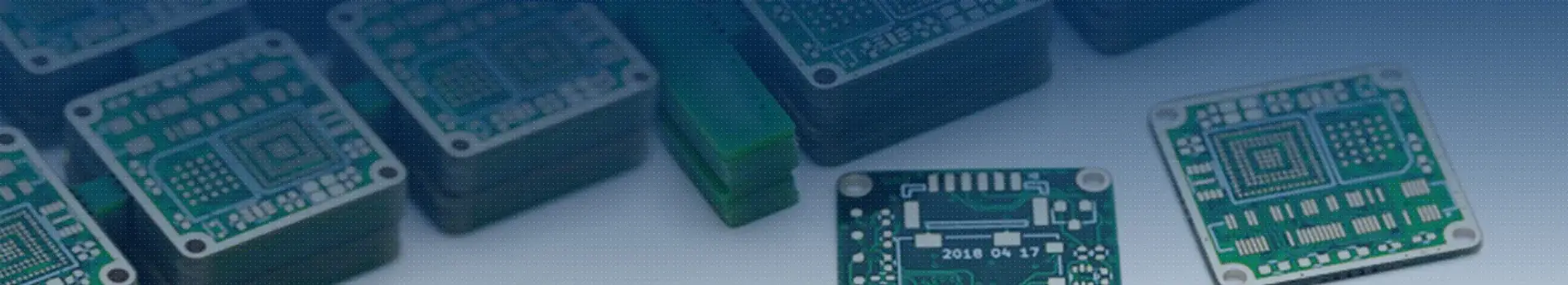
PCB制造

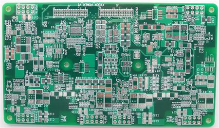
The following describes the use method and manufacturing steps of the light-sensitive pcb circuit board.

1、 Print:
Print the PCB drawing on the computer. The drawing software used by the author is prote198, the printer is Epson-580 ink-jet printer, and the printing paper is translucent sulfurIC acid paper. If there is a laser printer, the effect will be better if it is directly printed on the transparencies.
2、 Light insulation:
1. First, plan the light-sensitive PCB circuit board according to the required size, cut the protective film with scissors, cut the PCB circuit board with a saw or large scissors, and then polish the rough edges of the PCB circuit board with a file to prevent poor contact.
2. Remove the protective film. Paste the printed surface of the printed circuit diagram (carbon powder surface/ink surface) on the photosensitive film, and then press a piece of glass, which should be pressed tightly, and keep each contact surface clean and free of dirt to obtain the highest resolution.
3. Exposure time with various light sources.
1) Expose with 20W daylight lamp. The distance between the lamp tube and the glass plate is 5cm (15cm if 40W fluorescent lamp is used), and the standard time is 10 minutes (transparent film draft), 13 to 15 minutes (translucent sulfuric acid paper draft). If the width of the plate exceeds 10cm, two fluorescent lamps shall be used for average illumination.
2) Expose with sunlight. In strong sunlight outdoors, it takes 2 minutes for transparent film draft and 3 minutes for translucent sulfuric acid paper draft.
3) Expose with the strong light of the photo studio. It takes 1.5 minutes for transparent film draft and 2 minutes for translucent sulfuric acid paper draft.
3、 Imaging:
1. Prepare developer. The ratio of developer to water is 1:20. That is, one bag of 209 developer is mixed with 400ml of water. Note: the container should be a plastic basin, not a metal basin. The development solution can be prepared in proportion with the mineral water bottle so that it can be poured out at any time, but the used development solution cannot be poured back into the bottle.
2. Imaging: put the exposed sensitive plate film face up into the imaging solution, shake the container every few seconds until the copper foil is clearly visible and there is no green fog rising. At this time, wait a few seconds to confirm that the imaging is 100% complete. The imaging process takes about 1-2 minutes.
3. Flushing: Put the PCB circuit board under the tap and gently flush it.
4、 Corrosion:
1. Configuration of ferric chloride: 500g of blue ferric chloride is about 1500-2000ml of water, preferably hot water. Note that the container should be a plastic basin, not a metal basin.
2. Put the PCB circuit board into blue ferric chloride solution and stir it at any time for about 5~15 minutes to complete the corrosion.
3. Cleaning and drying: rinse the PCB circuit board with clean water, and then dry it with an electric hair dryer.
After the above steps, a beautiful printed PCB circuit board is ready, and components can be inserted and welded through the drilling eyebrow. The photosensitive film can be directly welded without removing. If it needs to be removed, it can be washed with alcohol.


抖音二維碼

Q Q二維碼

微信二維碼
點擊
然后
聯系
然后
聯系
電話熱線
13410863085Q Q

微信

- 郵箱