鑫景福致力于滿足“快速服務,零缺陷,輔助研發”PCBA訂購單需求。


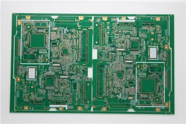
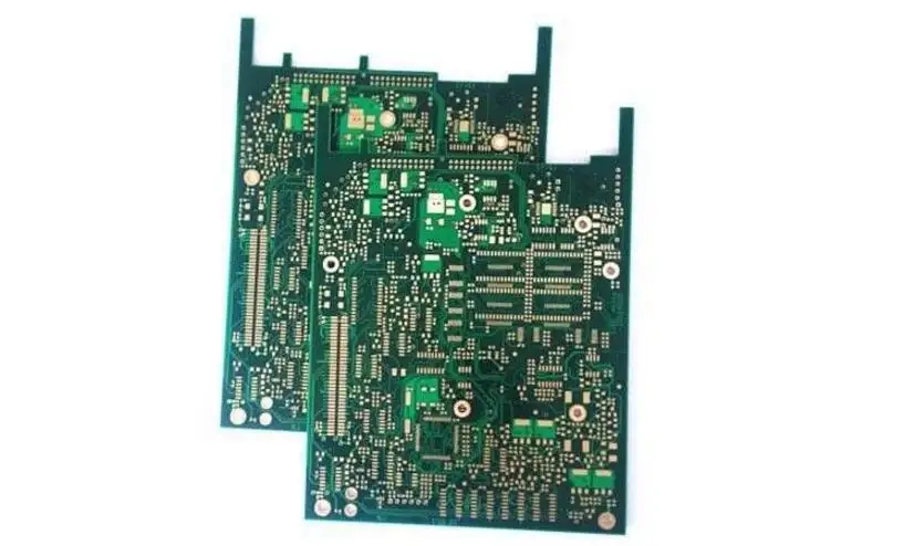
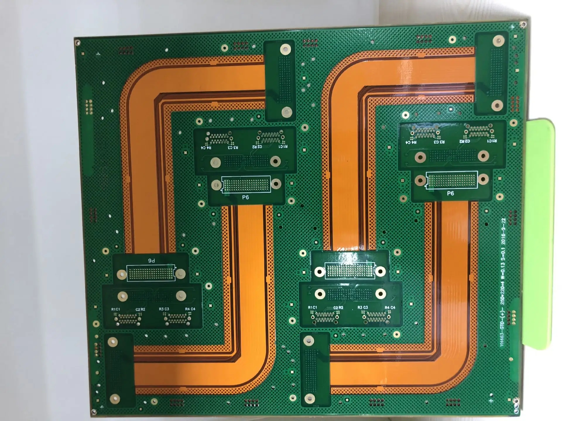
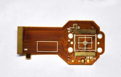
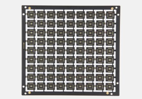
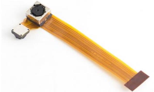
PCB制造
Under what circumstances can PCB be used without carrier wave soldering
PCB manufacturers and PCB designers will explain to you when PCB can be wave soldering without carrier
The design of printed circuit board is based on the circuit schematIC diagram to realize the functions required by the circuit designer. The design of printed circuit board mainly refers to layout design, which needs to consider the layout of external connections. The optimal layout of internal electronIC components, the optimal layout of metal wiring and through-hole, electromagnetic protection, heat dissipation and other factors. Excellent layout design can save production costs and achieve good circuit performance and heat dissipation. SIMple layout design can be realized by hand, while complex layout design needs to be realized by computer aided design (CAD).
Under what circumstances can PCB be used without carrier wave soldering
1、 PCB design requirements:
PCB shall reserve at least 5mm of plate edge for use of wave soldering chain and support when PCBA is placed in magazine.
The thickness of PCB should be more than 1.6mm, so that the problems of warpage and overflow will not occur when passing through the furnace.
It is recommended that the clearance distance of all welding pads should be more than 1.0mm to avoid short circuit between welding points.
2、 Requirements for parts and layout:
The type and direction of SMD parts must meet the requirements of wave soldering. (Generally speaking, SMD parts shall be perpendicular to the direction of plate travel)
The wave soldering surface of the circuit board only allows SMD parts, SOT, SOP, QFP, etc. with the size above 0603 (inclusive), and other parts such as BGA, PLCC, QFN, connector, transformer, 0402 (inclusive) cannot be placed on the wave soldering surface.
All plug-in parts must be designed on the first side and the direction of plug-in parts must meet the requirements of wave soldering. (The row pin must be parallel to the direction of board travel)
The parts on the PCB shall not be too heavy to avoid bending the circuit board due to gravity.
3、 Process requirements:
All SMD parts on the wave front soldering surface must be sprayed with red glue to avoid falling into the wave front soldering furnace.
Some solder pads (such as key contact lines and gold fingers) that cannot touch tin are not recommended to be designed on the wave soldering tin contact surface (the second side).
A few welding pads that cannot touch tin can be designed at the contact surface of the tin furnace, but the wave front welding must be pasted with high-temperature adhesive tape that will not residue, and the adhesive tape must be removed after completion. This design should be avoided as far as possible to reduce labor hours
All plug-in parts are recommended to use short legs for wave soldering to avoid short circuit. It is recommended that the leg length of the part should not exceed 2.54mm.

抖音二維碼

Q Q二維碼

微信二維碼
點擊
然后
聯系
然后
聯系
電話熱線
13410863085Q Q

微信

- 郵箱