鑫景福致力于滿足“快速服務,零缺陷,輔助研發”PCBA訂購單需求。


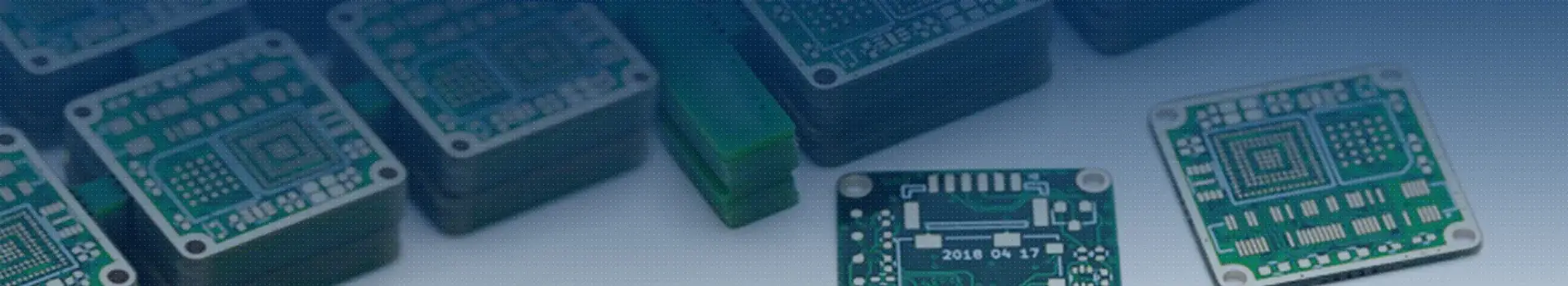
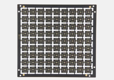
PCB制造

Five Little Experiences about PCB

1、 DevICe name:
If there are several versions of the circuit, or a circuit is revised before and after. For the same circuit part, the identification shall be the same before and after. Do not use R8 in one version and R9 in another.
In this way, when others (the object you serve) look at the first version, the impression and thinking of device naMES will not become invalid when they look at the second version. The continuity of thinking is very important. This also reduces the chance of making mistakes. Never use the automatic naming function of the software.
2、 Via
When designing IC, we often need to consider the parasitic of Via, mainly the resistance. However, when designing PCB, it was not considered before. Of course, our PCB layout engineers did not consider it.
The main power supply or other important places have decoupling and bypass capacitors. These capacitors should be placed next to the chip pins as much as possible, but they are often placed on the other side due to the location, so they need to pass through the vias. In some cases, we choose capacitors with low ESR/ESL, but a via often makes our money go to waste. Parasitic resistance of vias is often greater than line resistance.
Solution: It is better to put them on the same side. If they have to put them on the other side, the pins that enter the chip will come back through the vias from the next side. In this way, the parasitic resistance is the filtering effect.
However, it is hard to say how much improvement will be achieved if a capacitor is generated to a via resistance inside the chip. It seems that the ability to resist external interference has increased to a certain extent.
In addition, if more vias can be released, they should be released as much as possible, which will not increase the additional cost anyway. We often do this in IC design. On the one hand, the parasitic resistance is reduced, on the other hand, the reliability is increased, and the yield of production is increased.
3、 This is about the Production requirements
For resistors, we generally have no pipe direction. If we look at Japanese PCB boards, we often find that the color code direction of their resistors is the same. It will be convenient for others to look at, and we can tell how the company's management level is at a glance. The fact is that we usually have computers, and we can find out the products of this company by looking at the circuit boards of others.
4、 Lineweight
The signal line and power supply shall be as wide as possible.
5、 The pin sequence of schematic package and layout package should be consistent, which is convenient for comparison and reading, and is not easy to make mistakes.
Perhaps this problem is common sense in most design engineers. But we encountered this problem.
Over the years, great changes have taken place in PCB manufacturing process, which is due to the innovation of new technologies. These innovations enable circuit board manufacturers to innovate accurately and skillfully.
Accurately manufacturing PCB
1、 Front end engineering inspection
Before building a PCB prototype, there are countless aspects that can be used to plan the final result. First, the PCB manufacturer will carefully study the design of the circuit board (Gerber file) and begin to prepare the circuit board, which lists the manufacturing instructions listed step by step. After review, the engineer will convert these plans into data formats that are helpful for PCB design. The engineer will also check the format for any problems or clean-up.
This data is used to create the final circuit board and provide it with a unique tool number. This number tracks the PCB during construction. Even the SMAllest change to the board revision will result in a new tool number, which helps ensure that there is no confusion during PCB manufacturing and multi order manufacturing.
2、 Drawing
After checking the correct files and selecting the most suitable panel array, photo printing starts. This is the beginning of the production process. Photoelectric plotters use lasers to draw patterns, screens, and other major images on PCBs.
3、 Lamination and drilling
One of the three main types of printed circuit boards, multilayer PCB, requires lamination to fuse multiple layers together. This is usually done using heat and pressure.
After laminating the product, the professional drilling system will be programmed to drill accurately and accurately on the board. The drilling procedure ensures that there are no human errors during PCB manufacturing.
4、 Copper deposition and electroplating
Electrodeposited conductive copper layers are critical to the functionality of all prototype printed circuit boards. After electroplating, PCB formally becomes conductive surface, and copper is plated on the surface through electroplating solution. These copper wires are a conductive path connecting two points inside the PCB
PCB cleaning method
11-03,2022

抖音二維碼

Q Q二維碼

微信二維碼
點擊
然后
聯系
然后
聯系
電話熱線
13410863085Q Q

微信

- 郵箱