鑫景福致力于滿足“快速服務,零缺陷,輔助研發”PCBA訂購單需求。


PCB制造
Width setting standard of PCB process edge
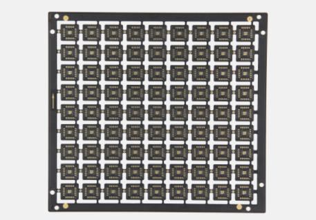
PCBA processing is to connect various electronIC components on PCB board through surface mount (SMT), plug-in (DIP) and other electronIC assemblies. PCBA process flow mainly includes SMT, AOI, DIP, FCT testing and other processes. Due to the size difference of electronic components, there will be different processes and requirements in assembly and insertion. The assembly density of PCBA is relatively high, and the SMAll size and light weight of electronic products also have certain changes and requirements in mounting. The reliability, seismic resistance and excellent weldability of the products have high requirements for the hardware and software facilities of PCBA processing.
In the PCB process flow, the process edge reservation is very important for the subsequent SMT chip processing. The process edge is the part that is added on both sides or four sides of the PCB to assist in the production of plug-in boards and welding peaks. It is mainly used to assist in production. It is not part of the PCB and can be removed after the completion of manufacturing and production. The main reason for leaving the process edge is that the SMT mounter track is used to clamp the PCB board and flow through the mounter. Therefore, components too close to the track edge will collide with each other when the SMT mounter nozzle absorbs the components and pastes them onto the pcb board. Therefore, a certain process edge, such as 2-5mm, must be reserved. SIMilarly, it is also applicable to some plug-in components to prevent similar phenomena during wave soldering.
Since the process side will consume more PCB boards, which will increase the overall cost of PCB, it is necessary to balance economy and manufacturability when designing PCB process side. For some PCB boards with special shapes, the original PCB boards with 2 or 4 process edges can be greatly simplified through panel assembly. When designing the splicing method, it is necessary to fully consider the track width of the SMT mounter. For the splicing method with a width of more than 350mm, it is necessary to communicate with the process engineer of the SMT supplier.
The flatness of PCB process edges is also an important part of PCB production, which is closely related to V-Cut. When removing PCB process edges, it is necessary to ensure that the process edges are flat. Especially for PCB boards with extremely high assembly accuracy requirements, any uneven burrs will lead to offset of the installation hole position, which will cause great trouble for subsequent assembly.
Circuit board assembly manufacturing
11-01,2022

抖音二維碼

Q Q二維碼

微信二維碼
點擊
然后
聯系
然后
聯系
電話熱線
13410863085Q Q

微信

- 郵箱