鑫景福致力于滿足“快速服務,零缺陷,輔助研發”PCBA訂購單需求。


行業新聞
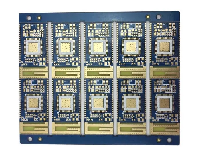
Introduction of vertICal plating through hole filling for pcb circuit board
For PCB with large thermal capacity, such as multilayer board or thick copper plate, proper and consistent hole filling is a challenge. It is important to ensure that these invisible defects do not become a catch, and that these plated holes are properly filLED with appropriate rework techniques.
Some common circuit board wiring or design may lead to incorrect or inconsistent hole filling, especially for PCBs with large thermal capacity. When the through hole is connected to the ground plate or the inner layer copper with greater weight, the thermal capacity of the element pin is higher than that of the surrounding pin. This means that it takes a long time for the circuit board to reach the correct return temperature. If the pin/hole does not reach the proper temperature, the solder in the hole has a low wettability, so it is not allowed to flow upward all the time.
In other wiring, the heat capacity distribution of each component pin may be uneven, which will have the same effect on hole filling. When more temperature sensitive devices are close to through-hole devices, this is another design challenge. The process engineer will "pull back" the temperature during wave soldering preheating to avoid damage to components. This lower temperature will cause the same hole to be underfilled. These are only some of the effects of design and wiring on hole filling.
Not only will the wiring and design of the circuit board lead to inconsistencies or poor hole filling, but also assembly and processing problems may lead to the same defects. A recent work shows that the selection of proper flux is one of the biggest factors affecting the hole filling in wave soldering process. The second major factor of improper hole filling is the poor permeability of flux to through-hole. Another source of improper hole filling is improper circuit board preheating and insufficient wave soldering dwell time. If the dwell time is too long, the copper plated holes will dissolve. If through hole reflow soldering is used instead of wave soldering or selective soldering, insufficient solder paste volume or inappropriate printing position may lead to improper hole filling. These and other process problems are more common causes of some process related hole filling defects.
Inappropriate hole filling requires appropriate inspection rules to detect defects. According to IPC A-610 standard, there are several methods to check whether the hole is filled correctly. Visual inspection can infer hole filling, but it must be confirmed by other methods of process capability analysis. For example, if there is annular wetting on both the source and target sides of a plated hole, it can be inferred that the hole is filled. The assembly process can be optimized and the filling amount of the electroplated through-hole can be measured by sectioning the cross section of the through-hole. This process can be confirmed to be under control by linking the amount of hole filling cross section with the visual inspection of the source and target pins and pads and the appropriate confidence interval.
X-ray inspection can use built-in algorithm to determine the hole filling percentage. Although the AOI system can detect the presence of source and target solder joints, they cannot determine whether there is solder in the hole.
Once defects are found and it is decided to rework the components, several rework processes can be used as part of the disposal of the circuit board. The addition of additional solder to the plated through-hole can take several different forms. In some cases, the solder fountain can fill the remaining part of the hole after proper preheating and adding proper flux. Care must be taken to ensure that the wave soldering dwell time is kept to a minimum, especially if copper dissolution may cause hole wall thinning or hole copper fracture. Heating the circuit board in the furnace before being affected by the peak temperature can reduce the thermal shock to the components while limiting the residence time. In the SIMplest case, a welding technician can solve the problem of insufficient hole filling through flux and soldering iron. If the circuit board has a large heat capacity, it must be preheated in a controlled furnace first. After being taken out of the furnace, flux and solder can be added to the hole immediately to fill the hole and meet the specification requirements.
Through careful process troubleshooting and understanding how the board wiring causes insufficient hole filling, appropriate rework process can be selected to make the hole filling meet the requirements.
PCB manufacturers, PCB designers and PCBA processors will introduce the filling of vertical electroplated through-hole of pcb PCB.


抖音二維碼

Q Q二維碼

微信二維碼
點擊
然后
聯系
然后
聯系
電話熱線
13410863085Q Q

微信

- 郵箱