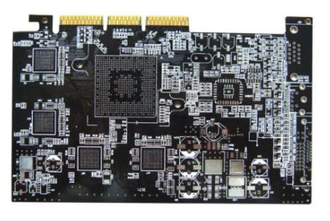

Summary of dry goods PCB drawing experience
<Strong>1. PCB design requirements
1. Correct
This is the most basIC and important requirement for PCB design It can accurately realize the connection relationship of power schematic diagram and avoid the two SIMple and fatal mistakes of "short circuit" and "open circuit" This basic requirement in manual design and PCB design using simple CAD software General products must go through more than two rounds of trial production and transformation More powerful CAD software has checking function to ensure the correctness of power connection
2. Reliable
This is a higher level requirement in PCB design A properly connected circuit board may not be reliable For example, the selection of circuit boards is unreasonable, the thickness and installation of boards are improper, the layout and wiring of components are improper, etc It may cause the printed circuit board to fail to work reliably, fail early, or even fail to work normally Another example is that multilayer boards are easier to design than single boards and dual boards, but they are not as reliable as single boards and dual boards From the perspective of reliability, the simpler the structure, the SMAller the surface, the fewer layers of circuit board, and the higher the reliability
3. Reasonable
This is a deeper and more difficult requirement in PCB design. The assembly of printed circuit board, from the manufacturing, inspection, assembly and debugging of printed circuit board to the assembly and debugging of the whole machine to the use and maintenance, is closely related to the rationality of printed circuit board, for example, poor shape selection, difficult processing, too small lead hole, difficult assembly, difficult to maintain the guiding height, and difficult to maintain the board connection correctly. Each difficulty may lead to new costs and longer working hours. Every difficulty stems from the designer's mistakes. There is no absolutely reasonable design, only the process of continuous rationalization. It requires the designer's sense of responsibility and rigorous style, as well as the experience of summarizing and improving in practice.
Printed circuit board

4. Economy
This is a goal that is not difficult to achieve, nor easy to achieve, but must be achieved. It is not difficult to say that it is not difficult to choose a low price for the circuit board, keep the size of the circuit board as small as possible, use direct welding wires for connection, use the cheapest surface coating, select the processing plant with the lowest price, etc., and the manufacturing price of the printed circuit board will drop. But don't forget that these cheap choices may lead to poor process and reliability, new manufacturing costs and maintenance costs, and the overall economy may not be able to handle them separately. In retrOSPect, this is not easy. "Must" is the principle of MARKet competition. The competition is cruel. Products with advanced principles and high technology may die for economic reasons.
PCB experience:
1. There must be a reasonable direction: such as input/output, AC/DC, strong/weak signal, high frequency/low frequency, high voltage/low voltage, etc. Their directions should be linear (or separate) and should not be mixed with each other. Its purpose is to prevent mutual interference. The best trend is a straight line, but it is usually not easy to achieve. The most unfavorable trend is round. Fortunately, isolation can be improved. The design requirements for DC, small signal and low-voltage printed circuit boards can be lower. So "reasonable" is relative.
Although there are some problems in the later production, they are caused by the design of printed circuit board. They are: there are too many vias, and a little negligence in the copper sinking process will lead to hidden dangers. This design shall minimize the wire holes. The density of parallel lines in the same direction is too large, which is easy to be connected together during welding. The linear density shall be determined according to the welding process level. The distance between welding points is too small, which is unfavorable to manual welding. The welding quality can only be solved by reducing the working efficiency. Otherwise, hidden dangers still exist. In this case, the minimum distance of welding spot shall be determined by comprehensively considering the quality and working efficiency of welding personnel. The size of the pad or via is too small, or the pad size does not match the hole size. The former is unfavorable to manual drilling, and the latter is unfavorable to numerical control drilling. It is easy to drill the liner into a "c" shape, but the liner must be drilLED out. The conductor is too thin, and there is no copper in a large area of the unwinding area, which is easy to cause uneven corrosion. That is, when the unwinding area is corroded, the thin wire may be excessively corroded, or may break or completely break. In this case, the setting function of copper is not only to increase the area of ground wire and anti-interference.
2. Protel Print Settings
The printing settings of SCH are relatively simple. Fill in all zeros in the upper left corner and lower right corner of the margin, and then click "Redraw", so that the page can be occupied within the maximum range, and the printed SCH image will be larger.
PCB setting: Open File>Set Printer... Set before printing.
In the printer setting menu that pops up, you must first select the printer: the first two are the default printers, and the last two are the printers we installed. One of the two tail codes is the final tail code, and the other is the composite tail code. The first means that the printer prints only one layer at a time, and the last one prints all the selected layers at a time. You can choose it according to your needs! Next: Click the option button below to set the content. Suppose you select final, and then enter the options you want to set. In general, you do not need to change the options after input. The scale is the printing scale, which is 1:1 by default. If you want to print a whole page, check this box! The performance hole on the right is very important. Select it to print the holes on the board. OK, click "Set" to set the paper size to complete the printer options. It's not over yet! Please go back to the dialog box used to select the contents of the printer, select the layer, and then set the printing layer. After entering, you can see it! Is it familiar? Select as needed.
3. Archives of Common PCB Library
1. The component library contained in the component library under the directory library pcb connectors contains most pcb packages of connector components
1) D-connector. Ddb, package software including parallel port and serial port interface components
2) Title. Ddb: package containing various plug components
2. The component library contained in the database in the library pcb generic footprints directory contains most of the printed circuit board
然后
聯系
電話熱線
13410863085Q Q

微信

- 郵箱


