鑫景福致力于滿足“快速服務(wù),零缺陷,輔助研發(fā)”PCBA訂購單需求。


PCBA方案設(shè)計
10 heat dissipation technologies in PCB circuit layout
The thermal sensor is placed in the cold air area
The temperature detector is placed at the hottest position.
Equipment PCBon the same equipment shall be arranged according to its calorifIC value and heat dissipation degree as far as possible Devices with SMAll computational value or poor heat resistance (such as small signal transistors, small integrated circuits, electrolytic capacitors, etc.) should be placed in cooling The superior flow (at the entry) of the air flow, and the devices with large heat generation or good heat resistance (such as power transistors, large scale integrated circuits, etc.) are placed at the most downstream of the cooling air flow
In the horizontal direction, high-power devices are arranged as close to the edge of the printed circuit board as possible to shorten the heat transfer path; In the vertical direction, high-power devices should be as close to the top of the printed circuit board as possible to reduce the impact of these devices on the temperature of other devices.
The heat dissipation of the printed board in the equipment mainly depends on the air flow. In this design, the air flow path should be studied and the equipment or printed board should be reasonably configured. When the air flows, it always tends to flow in the place with low resistance. When the equipment is instalLED on the printed circuit board, avoid leaving large space in specific areas. The same problem should also be paid attention to when multiple printed circuit boards are included in the whole machine.
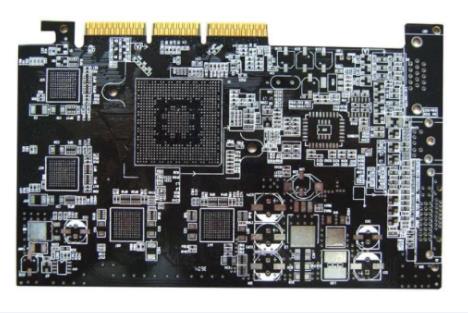
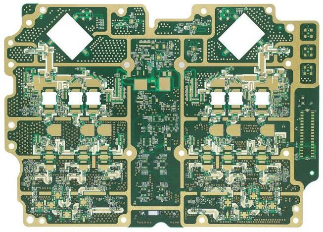
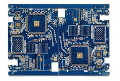
Circuit board

Temperature sensitive equipment should preferably be placed in the lowest temperature area (such as the bottom of the equipment). Do not place it directly above the heating device. It is better to stagger multiple devices on a horizontal plane.
Place the equipment with the highest power consumption and heat generation near the best heat dissipation position. Unless there is a radiator nearby, do not place high-temperature equipment at the corners and peripheral edges of the printed board. When designing power resistors, select larger devices as much as possible, and make them have enough heat dissipation space when adjusting the layout of printed boards.
Method II
When several components in a PCB generate a large amount of heat (less than 3), you can add a radiator or heat transfer tube to the heating component. When the temperature cannot be reduced, the radiator with fan can be used to enhance the cooling effect.
Radiator with fan
When the number of heating devices is large (more than 3), a large heat dissipation cover (plate) can be used, which is a special radiator customized according to the position and height of the heating device on the PCB. Or cut different component height positions on the large flat radiator.
The heat dissipation cover is buckled on the surface of the component as a whole and contacts with each component for heat dissipation. However, due to the poor high consistency during assembly and welding of components, the heat dissipation effect is not good. Generally, a soft thermal phase-change heat pad is added on the surface of the element to improve the heat dissipation effect.
Method 3
For equipment with free convection air cooling, it is better to arrange the integrated circuit (or other equipment) vertically or horizontally.
Method IV
Adopt reasonable wiring design to realize heat dissipation. Due to the poor thermal conductivity of the resin in the board, the copper foil wire and hole are good heat conductors. The residual rate of the newly added copper foil and the newly added heat conduction hole are the main means of heat dissipation.
It is necessary to calculate the equivalent thermal conductivity (nine eq) of the composite material composed of various materials with different thermal conductivity of the PCB
Method V
Components on the same PCB shall be arranged according to their calorific value and heat dissipation degree as far as possible. The equipment with low calorific value or poor heat resistance (such as small signal transistor, small integrated circuit, electrolytic capacitor, etc.) is placed on the top of the cooling airflow (inlet); Equipment with high heat or good heat resistance (such as power transistors), large-scale integrated circuits, etc.) are placed at the downstream of the cooling airflow.
Method VI
In the horizontal direction, high-power devices are arranged as close to the edge of the printed circuit board as possible to shorten the heat transfer path. In the vertical direction, high-power devices should be as close to the top of the printed circuit board as possible to reduce the impact of these devices on the temperature of other devices during operation.
Method 7
The heat dissipation of the printed board in the equipment mainly depends on the air flow. In this design, the air flow path should be studied and the equipment or printed board should be reasonably configured.
When the air flows, it always tends to flow in the place with low resistance. When the equipment is installed on the printed circuit board, avoid leaving large space in specific areas. The same problem should also be paid attention to when multiple printed circuit boards are included in the whole machine.
Method VIII
Temperature sensitive equipment should preferably be placed in the lowest temperature area (such as the bottom of the equipment). Do not place it directly above the heater. It is best to arrange multiple devices on a staggered horizontal plane.
Method 9
Place the equipment with the highest power consumption and heat generation near the best heat dissipation position. Unless there is a radiator nearby, do not place high-temperature equipment at the corners and peripheral edges of the printed board.
When designing power resistors, select larger devices as much as possible, and make them have enough heat dissipation space when adjusting the layout of printed boards.
Method X
Avoid the concentration of hot spots on the PCB, distribute the power evenly on the PCB as much as possible, and keep the PCB surface temperature efficiency uniform.
In the design process, it is usually difficult to achieve strict uniform distribution, but areas with high power density must be avoided to prevent hot spots from affecting the normal operation of the entire circuit If possible, it is necessary to analyze the thermal efficiency of the printed circuit For example, PCB design software for thermal efficiency quota analysis module has been added to some professional software to help designers optimize circuit design
The above is the explanation given by the editor of pcb circuit board company.
If you want to know more about PCBA, you can go to our company's home page to learn about it.
In addition, our company also sells various circuit boards,
High Frequency Circuit Board and SMT chip are waiting for your presence again.


抖音二維碼

Q Q二維碼

微信二維碼
點擊
然后
聯(lián)系
然后
聯(lián)系
電話熱線
13410863085Q Q

微信

- 郵箱