鑫景福致力于滿足“快速服務(wù),零缺陷,輔助研發(fā)”PCBA訂購單需求。


PCBA方案設(shè)計
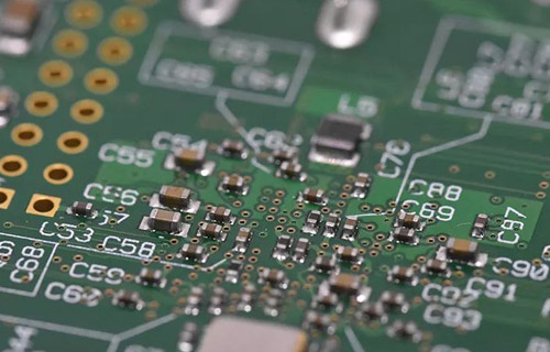
How to analyze timing in high-speed PCB design
For digital system design engineers, timing analysis is an important part of high-speed PCB design. Especially with the emergence of 100M bus, when the signal edge rate reaches the pICosecond level, the system performance depends on the front-end design, which requires accurate timing analysis and calculation at the beginning of the design. Timing analysis and signal integrity are inseparable, and good signal quality is the key to ensure timing relationship. The signal quality problems caused by reflection, crosstalk and other phenomena are likely to bring about timing offset and disorder, so we must consider the two together when designing.

The starting point of timing analysis is to determine the design scheme according to the signal establishment or holding time relationship. This method runs through the entire design process, including IC design, board level design and system design. Flight time refers to the difference between the time when the signal is sent and the time when the signal is stable at the receiving end, which is used to describe the delay caused by wiring and load. In the case of low speed, approximate method can be used to determine, but in the design of high-speed PCB, due to the influence of load, transmission line effect and other factors, SIMulation method must be used to determine. After the flight time is determined, the timing calculation can be realized by table or manual method to check whether the signal meets the signal sampling and holding requirements. Similarly, reverse this process to obtain wiring length rules. The common clock mode is characterized by that the clock at the receiver and transmitter is provided by the common clock source. It has two characteristics: first, it requires data to reach the receiver within one cycle, and second, the clock difference has a great impact on the timing.
Generally, when the clock and data are driven by the same type of interface, timing calculation only needs to consider the difference between them. If this is not the case, the difference (such as wiring length) needs to be adjusted according to the flight time. At this time, the data clock wiring method of equal length in the general sense in PCB design becoMES invalid. In the design, other factors such as switching noise, intersymbol interference, and non ideal circuit have influence on the signal phase. Therefore, on the one hand, we should reasonably add design margin in timing design, on the other hand, we need to use other design methods to reduce the impact of interference.


抖音二維碼

Q Q二維碼

微信二維碼
點擊
然后
聯(lián)系
然后
聯(lián)系
電話熱線
13410863085Q Q

微信

- 郵箱