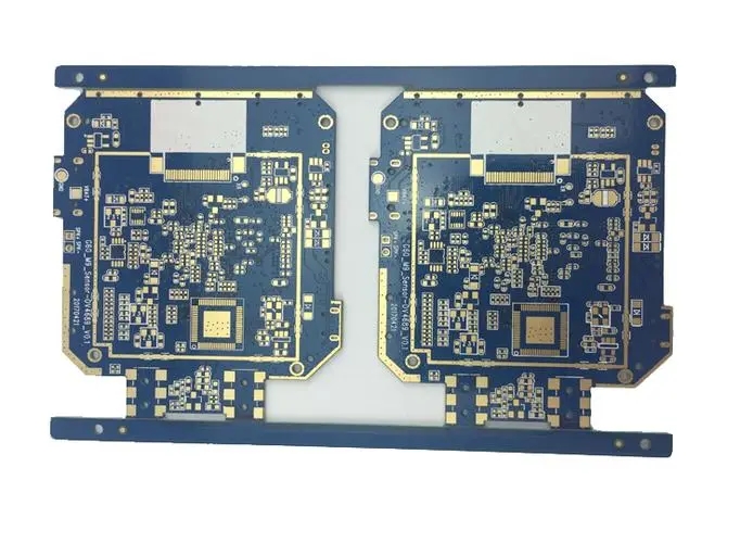
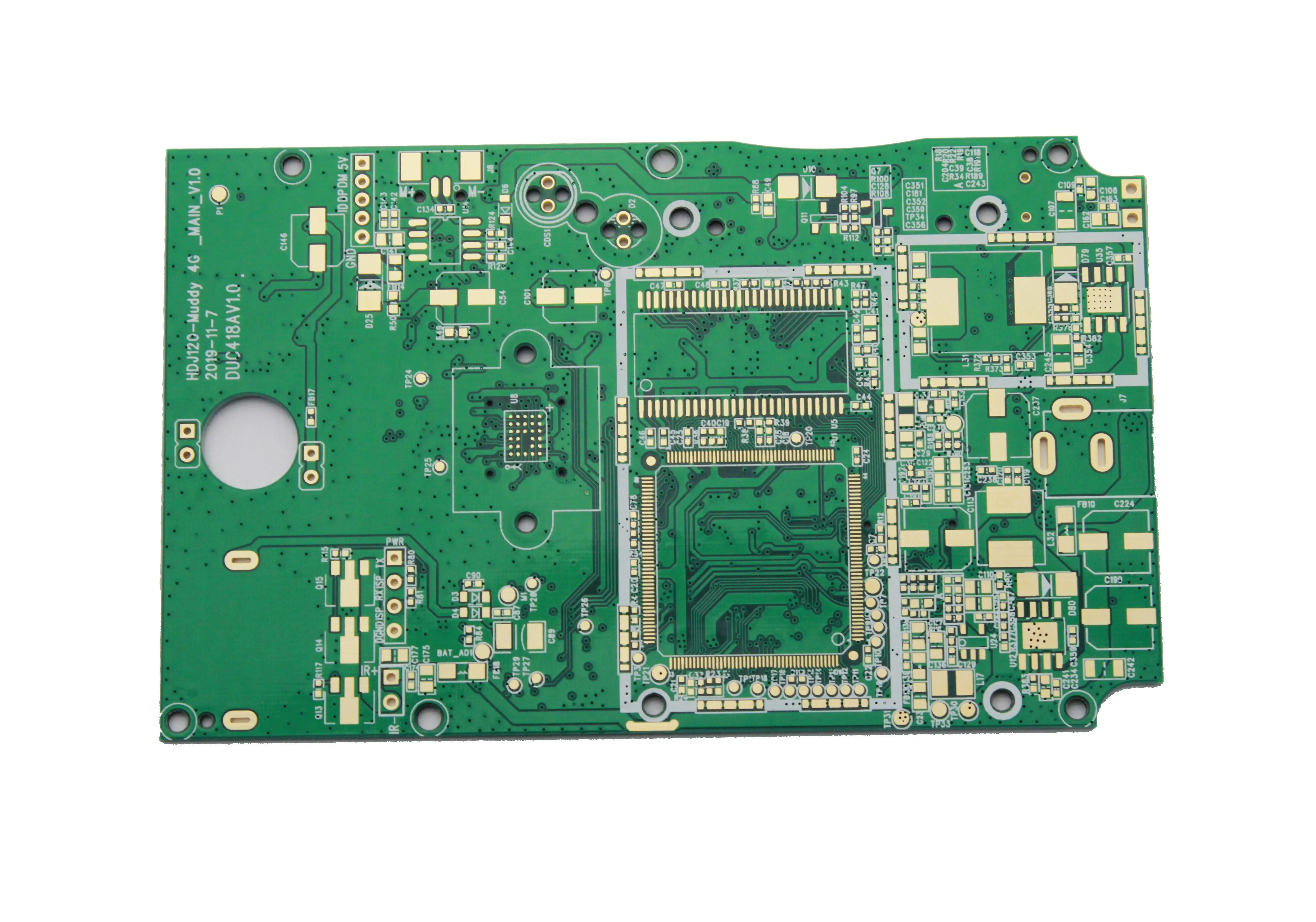
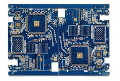
鑫景福致力于滿足“快速服務,零缺陷,輔助研發”PCBA訂購單需求。


PCBA方案設計
PhysICal design Analysis of PCB in Switching Power Supply Design
In the design of switching power supply, the physical design of PCB board is the last link. If the design method is improper, PCB may radiate too much electromagnetic interference, causing instability of power supply. The following is an analysis of matters needing attention in each step:
1、 Create component parameters from schematic diagram to PCB design process ->Input schematic network table ->Design parameter setting ->Manual layout ->Manual wiring ->Validate design ->Review ->CAM output.
2、 The spacing between adjacent conductors in parameter setting must meet the electrical safety requirements, and the spacing should be as wide as possible to facilitate operation and production. The minimum spacing shall at least be suitable for the voltage. When the wiring density is low, the spacing of signal lines can be appropriately increased. The signal lines with high and low level differences shall be as short as possible and the spacing shall be increased. Generally, the wiring spacing is set to 8mil.
The distance from the edge of the inner hole of the pad to the edge of the printed board shall be greater than 1mm, so as to avoid pad defects during processing. When the wiring connected with the pad is thin, the connection between the pad and the wiring should be designed as a water drop. This has the advantage that the pad is not easy to peel, but the wiring and the pad are not easy to disconnect.
3、 The practice of component layout has proved that even if the circuit schematic diagram is correctly designed and the printed circuit board is improperly designed, the reliability of electronic equipment will be adversely affected. For example, if two thin parallel lines of the printed board are close together, the delay of the signal waveform will be formed and the reflected noise will be formed at the end of the transmission line; The interference caused by improper consideration of power supply and ground wire will degrade the performance of the product. Therefore, correct methods should be used when designing printed circuit boards. Each switching power supply has four current circuits:
(1)。 AC circuit of power switch
(2)。 Output rectifier AC circuit
(3)。 Input signal source current loop
(4)。 The output load current loop and the input loop charge the input capacitor through a DC current, and the filter capacitor mainly plays a broadband energy storage role; SIMilarly, the output filter capacitor is also used to store high-frequency energy from the output rectifier and eliminate the DC energy of the output load circuit. Therefore, the terminals of the input and output filter capacitors are very important. The input and output current circuits should be connected to the power supply only from the terminals of the filter capacitors; If the connection between the input/output circuit and the power switch/rectifier circuit cannot be directly connected to the terminal of the capacitor, the AC energy will be radiated to the environment by the input or output filter capacitor. The AC circuit of the power switch and the AC circuit of the rectifier contain high amplitude trapezoidal currents. The harmonic component of these currents is very high, and its frequency is far greater than the basic frequency of the switch. The peak amplitude can be up to 5 tiMES the amplitude of the continuous input/output DC current. The transition time is usually about 50ns. These two circuits are most likely to generate electromagnetic interference, so these AC circuits must be laid before wiring other printed lines in the power supply. The three main components of each circuit, filter capacitor, power switch or rectifier, inductor or transformer, should be placed adjacent to each other. Adjust the component position to make the current path between them as short as possible. The best way to establish the switching power supply layout is similar to its electrical design. The best design process is as follows:
Place the transformer
Design power switch current circuit
Design current circuit of output rectifier
Control circuit connected to AC power circuit
Design input current source circuit and input filter Design output load circuit and output filter According to the functional unit of the circuit, the layout of all components of the circuit shall comply with the following principles:
(1) First, consider PCB size. When the PCB size is too large, the printed line is long, the impedance increases, the noise resistance decreases, and the cost increases; If it is too SMAll, the heat dissipation is poor, and adjacent lines are vulnerable to interference. The optimal shape of the circuit board is rectangular, with a length to width ratio of 3:2 or 4:3. The distance between the components located at the edge of the circuit board and the edge of the circuit board is generally not less than 2mm. (2) When placing the device, it is necessary to consider the future welding, not too intensive.
(3) Take the core components of each functional circuit as the center, and arrange around it. The components and parts shall be evenly, orderly and compactly arranged on the PCB to minimize and shorten the lead and connection between components and parts, and the decoupling capacitor shall be close to the VCC of components as much as possible.
(4) For circuits operating at high frequencies, the distribution parameters between components should be considered. For general circuits, components shall be arranged in parallel as far as possible. In this way, it is not only beautiful, but also easy to assemble and weld, and easy to mass produce.
(5) Arrange the position of each functional circuit unit according to the circuit flow, so that the layout is convenient for signal flow and the signal is kept in the same direction as far as possible.
(6) The primary principle of layout is to ensure the distribution rate of wiring, pay attention to the connection of flying wires when moving components, and put the components with wiring relationship together.
(7) Reduce the loop area as much as possible to suppress the radiated interference of switching power supply.
4、 The wiring switching power supply contains high-frequency signals. Any printed wire on the PCB can act as an antenna. The length and width of the printed wire will affect its impedance and inductance, thus affecting the frequency response. Even the printed wire passing through the DC signal will be coupLED to the RF signal from the adjacent printed wire and cause circuit problems (or even radiate interference signals again). Therefore, all printed wires passing through AC current should be designed as short and wide as possible, which means that all components connected to the printed wire and other power lines must be placed close together. The length of the printed wire is proportional to its inductance and impedance, while the width is inversely proportional to its inductance and impedance. The length reflects the wavelength of the printed wire response. The longer the length is, the lower the frequency of the printed wire that can send and receive electromagnetic waves, and it can radiate more RF energy. According to the current of the printed circuit board, try to rent the width of the power line to reduce the loop resistance. At the same time, make the direction of the power line and ground wire consistent with the direction of the current, which helps to enhance the anti noise ability. Grounding is the bottom branch of the four current loops of switching power supply, which plays an important role as the common reference point of the circuit and is an important method to control interference. Therefore, the placement of grounding wires should be carefully considered in the layout. Mixing various grounding wires will cause unstable power supply.
Attention shall be paid to the following points in the design of ground wire:
1. Correct selection of single point grounding Generally, the common terminal of the filter capacitor should be the only connection point for other grounding points to couple to the high current AC ground. The grounding point of the same level circuit should be as close as possible, and the power filter capacitor of this level circuit should also be connected to the grounding point of this level, mainly considering that the current returned from each part of the circuit to the ground is variable, The impedance of the line actually flowing through will lead to the change of the ground potential of each part of the circuit and introduce interference. In this switching power supply, its wiring and inductance between components have less influence, while the circulating current formed by the grounding circuit has greater influence on the interference, so one point grounding is adopted, That is, the power switch current circuit (the ground wires of several components in the circuit are connected to the grounding pin, and the ground wires of several components in the current circuit of the output rectifier are also connected to the grounding pin of the corresponding filter capacitor, so that the power supply works more stably and is not easy to self excite. If a single point cannot be achieved, connect two diodes or a small resistance at the common ground, which can be connected to a relatively concentrated copper foil.
2. thicken the grounding wire as much as possible. If the grounding wire is very thin, the grounding potential will change with the change of current, resulting in unstable timing signal level of electronic equipment and poor anti noise performance
PCB manufacturers, PCB designers and PCBA manufacturers will explain the physical design analysis of PCB in switching power supply design.


抖音二維碼

Q Q二維碼

微信二維碼
點擊
然后
聯系
然后
聯系
電話熱線
13410863085Q Q

微信

- 郵箱