鑫景福致力于滿足“快速服務(wù),零缺陷,輔助研發(fā)”PCBA訂購單需求。


PCBA方案設(shè)計
Explain the key points of PCB design of differential line pair
Differential line pair refers to a pair of transmission lines with coupling. Differential signal transmission uses two output drives to drive the differential line pair, one carries the signal, and the other carries its complementary signal. What we need is the voltage difference between differential line pairs, whICh carries the information to be transmitted.
Differential signal transmission has many advantages over single ended signal transmission:
① Strong anti-interference capability, because the coupling between the two differential lines is very good, when there is noise interference from the outside, it is almost coupLED to the two lines at the same time, and the receiver only cares about the difference between the two signals, so the external common mode noise can be completely offset;
② It can effectively suppress EMI. In the same way, since the polarities of the two signals are opposite, the electromagnetic fields radiated by them can cancel each other. The closer the coupling is, the less electromagnetic energy is released to the outside world;
③ The timing positioning is accurate. Because the switch change of the differential signal is located at the intersection of two signals, rather than relying on the high and low threshold voltages to judge the single ended signal, it is less affected by the process and temperature, which can reduce the timing error, and is more suitable for the circuit design of low amplitude signals.
For PCB engineers, the most important thing is to ensure that the advantages of differential signal can be fully utilized in actual wiring. People who have been exposed to PCB design will understand the general requirements of difference distribution lines, that is, "equal length, equal distance". However, all these rules are not used to copy mechanically. Many engineers do not seem to have made in-depth analysis on the actual design of differential line pairs. Here are some common points in PCB differential signal PCB design.
1 Equal length
Equal length is to make the signal transmission delay on each line the same, so as to ensure that the two differential signals always maintain opposite polarity. Any delay difference between the two transmission lines will change some differential signals into common mode signals, which will seriously affect the signal quality.
Equal length is to make the wiring length of the two signal lines of the differential line pair as same as possible. Generally, the matching requirement for equal length of high-speed differential signal is within ± 10 mils. Of course, this is a high requirement. The true value can be calculated by the allowable signal misalignment (skew, which can be found in the chip manual) and the signal transmission delay (generally 180 picoseconds per inch).
Due to device layout, pin distribution and other reasons, the differential lines generated by direct wiring are not equal in length in most cases, which requires manual winding. Manual winding is generally carried out at the chip pin to reduce the differential line to impedance discontinuity. Figure 1 shows two common winding methods.
2 equidistant
Isometric is to ensure the continuity of differential impedance between differential line pairs and reduce reflection. Differential impedance is an important parameter for designing differential pairs. If it is discontinuous, signal integrity will be affected. The differential impedance can be regarded as the equivalent impedance of two single ended signal lines in series. Generally, the equivalent impedance of single ended signal lines is 50 ?, so the differential impedance should be kept at 100 ? in general. Equidistant means to keep the distance between the differential line pairs equal (i.e. parallel routing), so as to ensure that the differential impedance of the differential line pair does not change in the whole process.
The differential impedance is related to many parameters such as the line width, line spacing, stacking sequence of printed boards, dielectric constant of the medium, etc. of the differential line pair. Some parameters can only be provided by the printed board manufacturer. Therefore, the printed board designer should negotiate with the manufacturer to determine the parameters such as line spacing. It is worth noting that when a differential signal is transmitted at different layers of a multilayer PCB (especially when both the inner and outer layers are wired), the line spacing should be adjusted in time to compensate for the change in characteristic impedance due to the change in dielectric constant of the medium. Compared with unequal length, unequal distance has less influence on signal integrity. When the equal length rule conflicts with the equal distance rule, the equal length rule shall prevail.
3 Differential line pair and printed board lamination
The stack setting of PCB board is closely related to signal coupling and shielding. There is a view that differential line pairs provide each other with a return path, so differential signals do not need the ground plane as a return path, which is a wrong understanding. Generally, the coupling between differential lines is relatively SMAll, accounting for only 10%~20% of the coupling degree, and more coupling to the ground. Therefore, the main return path of differential lines still exists in the ground plane. In PCB design, differential signal is required to be close to at least one ground plane, and it is best that both sides can be close to ground plane. Stacking mode is recommended. The signal quality decreases from left to right, but it can meet the basic requirements. Like the high-speed single ended line, the differential line pair also requires the integrity of the reference ground plane. That is, the reference ground plane of the differential line pair on the path must be continuous without division.
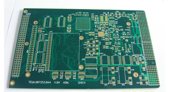
PCB manufacturers, PCB designers and PCBA manufacturers explain the PCB design points of differential line pairs


抖音二維碼

Q Q二維碼

微信二維碼
點擊
然后
聯(lián)系
然后
聯(lián)系
電話熱線
13410863085Q Q

微信

- 郵箱