鑫景福致力于滿足“快速服務,零缺陷,輔助研發”PCBA訂購單需求。


PCBA方案設計
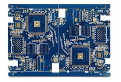
Relationship between layout and switching power supply of PCB board
Due to the switching characteristICs of switching power supply, switching power supply is prone to generate large electromagnetic compatibility interference As a power supply engineer, electromagnetic compatibility engineer, or PCB layout engineer, you must understand the causes of electromagnetic compatibility problems and take measures. Especially, layout engineers need to know how to avoid the spread of stains
The main points of the power supply PCB discussed the design
2.9 Layout and PCB board
1. Several basic principles: any conductor has impedance; The current always automatically selects the path of impedance; Radiation intensity is related to current, frequency, and loop area; Common mode interference is related to the mutual capacitance of large dv, and the/dt signal is grounded; The principle of reducing electromagnetic interference is SIMilar to that of enhancing anti-interference capability
2. The layout shall be divided according to power supply, analogy, high-speed digital and each functional block
3 Minimize the area of large di/dt loop and reduce the length (or area, width of large dv/dt signal line) The new trace area will add distributed capacitance The general method is: the width of the trajectory should be as large as possible, but remove the excess part), try to walk in a straight line, and reduce the hidden closed area to reduce radiation
4 Inductive crosstalk is mainly caused by large di, so it is more important to reduce the mutual inductance with these signals (the main way is to reduce the loop area and increase the distance); Sequal crosstalk is mainly generated by large dv/dt signal, and the induction is proportional to the mutual capacitance All decrease the mutual capacitance with these signals (the main way is to reduce the effective coupling area and increase the distance. Faster) is more critical
5. Try to use the loop cancellation principle to route, and further reduce the large area di/dt loops (similar to twisted pair, use the principle of loop cancellation to improve anti interference ability and increase transmission distance)
PCB board

6. Reducing the loop area can not only reduce the radiation, but also reduce the loop inductance, making the circuit more efficient
7. To reduce the loop area, we need to design the return path of each track
8. When multiple PCB boards are connected through connectors, it is also necessary to consider making the loop area reach, especially for large di/dt signals, high-frequency signals or sensitive signals The signal wire corresponds to the ground wire, and the two wires are as close as possible Twisted pair wires can be used to connect (the length of each twisted pair wire responses to an integral multiple of the noise half wavelength) if necessary If you open the computer host shell, you can see that the USB interface from the host board to the front panel is connected by twisted pair It can be seen that twisted pair connection is very important for anti-interference and reducing radiation
9. For data cable, try to arrange more ground wires in the cable and make them evenly distributed in the cable, which can effectively reduce the loop area
10. Because these low frequency signals contain a lot of high frequency noise (through conduction and radiation), even though some connecting lines between boards are low frequency signals
11. When wiring, first consider the traces of high current and vulnerable to radiation
12. The switching power supply usually has four current circuits: input, output, conversion and free riding Among them, the input and output current loops are almost DC, hardly generating electromagnetic interference, but they are easy to be interfered; The switch and freewheeling current loop have large di/dt, which should be noted
13. The gate drive circuit of the mos (igbt) tube usually also contains a large di/dt.
14. Do not place SMAll signal circuits, such as control and analog circuits, high internal current, and high-frequency and high-voltage circuits that interfere
15. Reduce the susceptible (sensitive) signal loop area and trace length to reduce interference.
16. The trace of small signals is far from large dv/dt signal lines (such as the C pole or D pole of the switch tube, buffer (snubber) and clamp network) to reduce coupling, and ground (or power supply, in short, soft potential signal) to further reduce the coupling At the same time, small signal traces should be as far away from dt signal lines with large di/inductive crosstalk prevention as possible Do not track small signals/dt signal under large dv If the back of the small signal traces can be ground (the same ground)
17. A better method is to lay ground/dt and di/dt signal tracks (including the C/D poles of the switching devices and the switch tube heat sink) around and on the back of these large dvs, and use the upper and lower layers for grounding Connect this ground to a common ground point (usually the E/switch S pole, or sampling resistor) with a low impedance trace This reduces radiated EMI It should be noted that the small signal grounding should not be connected to the shield grounding, otherwise greater interference will be generated Large dv/dt trajectories usually interfere with the radiator and nearby ground through mutual capacitive coupling Connect the switch tube radiator to the hood ground The use of surface mount switching devices will also reduce mutual capacitance, thereby reducing coupling
18. For easily disturbed traces, do not use vias, because they will interfere with all layers through which the vias pass
19. The mask can reduce the radiated EMI. However, due to the new capacitance to ground, the conducted EMI (common mode, or external differential mode) will increase. As long as the mask layer is properly grounded, it will not increase too much. It can be weighed and considered in the actual design
20. Prevent common impedance interference, and use one point grounding and one point power supply
PCB board
21. The switching power supply usually has three grounds: input power supply high current ground, output power high current ground, and small signal control ground The ground connection method is shown in the following diagram:
22. When grounding, first judge the nature of the ground, and then connect it The grounding of sampling and error amplification should normally be connected to the negative pole of the output capacitor The sampling signal shall normally be selected from the positive pole of the output capacitor Common impedance interference Generally, the control grounding and drive grounding of integrated circuits are not LED out separately At this time, the lead impedance from the sampling resistor to the ground must be as small as possible to reduce the common impedance interference and improve the accuracy of current sampling
The output voltage sampling network is close to the error amplifier rather than the output This is because low impedance signals are less susceptible to interference than high impedance signals The sampling track should be as close as possible to reduce picked up noise
24. It shall be noted that the inductance shall be arranged far away and perpendicular to each other to reduce mutual inductance, especially energy storage inductance and filter inductance
25. When the high-frequency capacitor and low-frequency capacitor are used in parallel, pay attention to the layout. The high-frequency capacitor is close to the user
26. Low frequency interference is generally different mode (below 1M). High frequency interference is usually common mode, usually coupled by radiation
27. If the high-frequency signal is coupled to the input wire, it is easy to form EMI (common mode) You can place a magnetic ring on the input wire near the power supply If the electromagnetic interference is reduced, this indicates the problem The solution to this problem is to reduce the circuit coupling or EMI If the high-frequency noise is not filtered and transmitted to the input wire, EMI (differential mode) will also be formed At this point, the magnetic ring cannot solve this problem String two high-frequency inductors (symmetrical) where the input lead is close to the power supply. A drop indicates the problem The solution to this problem is to improve filtering, or reduce high-frequency noise generation, clamping and other pipes by buffering
28. Measurement of differential mode and common mode current
29. The EMI filter shall be as close to the incoming line as possible, and the wiring of the incoming line shall be as short as possible to minimize the coupling between the front and rear stages of the EMI filter The incoming line is shielded with the chassis ground (the method is as described above). The output EMI filter shall be treated similarly Try to increase the distance between the incoming line and the high dv/dt signal traces, which should be in the PCB layout
The above is the explanation given by the editor of pcb circuit board company.
If you want to know more about PCBA, you can go to our company's home page to learn about it.
In addition, our company also sells various circuit boards,
High Frequency Circuit Board and SMT chip are waiting for your presence again.


抖音二維碼

Q Q二維碼

微信二維碼
點擊
然后
聯系
然后
聯系
電話熱線
13410863085Q Q

微信

- 郵箱