鑫景福致力于滿足“快速服務(wù),零缺陷,輔助研發(fā)”PCBA訂購單需求。


PCBA方案設(shè)計
Line width and copper thICkness in PCB design
1. Relationship between copper and platinum thickness, line width and current PCB design
Before the PCB board was designed with copper platinum, line width and current, let's first understand that the conversion relationship between inch and millimeter of PCB and copper thickness of PCB is. 0014 inch=. 03.56 mm, 2 ounce=0.0028 inch=0.0712 mm, and ounce is. The reason why it can be converted to millimeter is Copper
thickness is ounce/square inch. "This design is about copper platinum thickness, line width, and the relationship between PCBs. 15× Line width (W) =A. The above data is, Wire 0005&TImes; L/W, current carrying capacity direct/pad and via on the line Inside, the current carrying value of the conductor is equal to that of the conductor There is a direct relationship between the current carrying value wire and the number of vias of the wire and the number of pads (currently, no calculation. Interested friends can pass through. I am not very clear, so I will not explain.) Here are just a few SIMple main factors that affect the current carrying value of the line
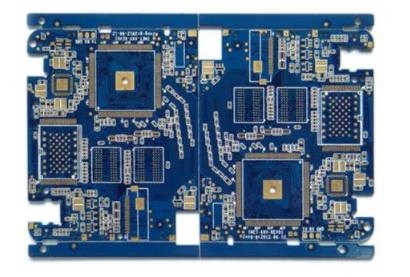
PCB board
Bearing values listed in 1.1 Therefore, various factors, such as manufacturing technology, plate process, and design So, this one
1. It is actually designed as 2, and each wire will also be affected by the pad and via. For example, after tin plating, there may be many current carrying The reason is very simple There are component pins on the pad and solder after soldering, which enhances the current carrying capacity of this section Pad current carrying value between pads and Therefore, it is easy to burn when the circuit is subject to transient fluctuations Solution: Add new wires If the circuit board cannot allow additional wire width, add a Solder layer (generally 1 mm A wire of about 0.6 welding layer is OK, of course, you also add a 1mm Solder layer wire) So after tinning, the 1mm wire (depending on the wire) The uniformity of tin and the amount of tin when tin is passed), as shown in The figure below: the relationship between PCB design and current Not familiar, so if the tin content is uniform, 1 mm wire can exceed 2 mm wire This is very important in single-sided high current plates
1.3 This is especially true in the boards with large current and thick pins (the pins are greater than 1.2 and the pads are more than 3). important. Because if the cushion is larger than 3mm, the pin is larger than 1.2 If, the current of the entire line The carrying capacity will be very unexpected (especially when there are many pads) This Again: the If it is not a design, add 10% design requirements based on the data provided in the table In general single panel design, this can basically be the ratio of designed ed, that is, 1A current can be designed with 1mm conductor, which can meet the requirements (calculated at a temperature of 105 degrees)
PCB board
2. Relationship between copper foil thickness, trace width and current input PCB design
This When the average current of the signal, the current that can be carried by the wiring width shall be The line width can refer to the following data: design of the PCB, this, different PCB designs
Note: 2.1 Current carrying capacity of copper foil when copper is used as conductor 2.2 inch design and PCB processing, OZ is commonly used as the organization of copper thickness 1 ounce of copper, equivalent to a physical thickness of 35um; 2OZ copper
3. How to determine the line width of large current wires
The Relationship between Line Width and Copper Platinum Thickness and Current PCB Design
The relationship between line width and copper plate thickness and current in PCB design
4. The used temperature impedance calculation software PCB to calculate (calculate the line width, current, impedance, etc.) Very convenient. In PCB design, you can see that the results of the same method are similar (20 degrees Celsius, 10 mil line width, 0.010 inch line width, copper foil thickness is 1 Oz)
5. Empirical formula
I=KT0.44A0.75 (K is the correction factor Normally. 010inch=0.254 can be 1A, 250 mils=6.35 mm, now it is 8 points. 3A
6. A little experience about line width and copper paving
When drawing PCB boards, we usually have a common sense: use thick lines (such as 50 mils or more) where large currents are used, and thin lines (such as 10 mils) can be used for low current signals For, sometimes it is instantaneous, so the thinner it is The basic empirical value is:/mm2, that is, with If the current is high, the circuit will burn out Of course, the current burned trace must also follow the energy formula: Q=I * I * t (At this time, the actual length of the wire must be considered) General PCB drawing software usually has several, 45 degree spokes, and direct laying What is it? Novice usually don't care much, just choose Actually not There are mainly two kinds, the other one This method must be used for At the same time, its thermal conductivity is also very high Although it is beneficial to heat dissipation of equipment, this is a problem for circuit board solders Because the heat dissipation of the cushion is too fast, it is not easy. Generally, higher power welding is required The use of right angle spokes and 45 angle spokes will reduce contact, slow heat dissipation, and Therefore, the copper connection is selected as well as the whole Do not use direct routing for low-power signals. For pads passing high current, they must be straight Shop. At right angles or 45 degrees, it looks good Why? Because I have been making a motor driver, the H-bridge component in the driver is always burnt out. I can't find the reason for four to five years After a lot of efforts, I finally found out: It turned out that the pad of a device in the power circuit was coated with right angle cookies (and because of the power cookie painting, only two cookies actually appeared) Here Although the product has no problems during normal use, it is However, when the current of about 100A appears on the display screen, and the two sparks will be burned instantaneously (uS level) The power circuit then becomes open and stored energy This energy will burn the current measuring resistor and destroy the bridge control It penetrates into digital signal and power supply, causing serious damage to PCB equipment of the whole system


抖音二維碼

Q Q二維碼

微信二維碼
點擊
然后
聯(lián)系
然后
聯(lián)系
電話熱線
13410863085Q Q

微信

- 郵箱