鑫景福致力于滿足“快速服務(wù),零缺陷,輔助研發(fā)”PCBA訂購單需求。


PCBA方案設(shè)計

pcb board design principles for reducing electromagnetIC interference
The effective anti-interference design of PCB is to design electronic products, which affects the reliability and stability of circuit operation This paper analyzes the main causes of electromagnetic interference on the circuit board, and summarizes the effective suppression and prevention methods of electromagnetic interference. PCB design includes the selection of circuit board, the layout of circuit board components, the wiring of power supply and grounding, and the wiring of signal lines Measures and principles Printed circuit board is the carrier of circuit components in electronic products. It provides electrical connection between circuit components and is the basic component of various Electronic devices Its efficiency is directly related to the quality of electronic equipment With the development of information age and electronic technology, the integration of circuits is getting higher and higher, the size of circuit boards is getting SMAller and smaller, the density of components on circuit boards is getting higher and higher, and the operation speed of electronic products is getting faster and faster Therefore, the electromagnetic interference and compatibility problems caused by itself are more prominent Therefore, how to reduce the EMI of PCB has become a hot topic in today's electronic technology The electromagnetic compatibility of the circuit board is the key to the normal operation of the electronic system, which affects the reliability and stability of the circuit or system Therefore, the electromagnetic interference problem should be effectively solved under the following conditions: design the inertial navigation and guidance PCB board
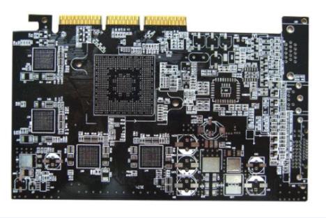
PCB board

With regard to the causes of electromagnetic interference, the measures and principles for reducing electromagnetic interference that should be considered are summarized in PCB design
1. This reason for the existence of electromagnetic interference on the circuit board
In the high speed electronic system composed of switching power supply and microprocessor, the electromagnetic interference of the circuit board mainly coMES from existing radio frequency interference sources, components, basic loops, differential mode and common mode noise
1.1 This source of radio frequency interference present on the circuit board
In an intelligent high-speed electronic system, the RF interference sources on the circuit board mainly come from the microprocessor system, power supply system and oscillator circuit
1) Microprocessor system
The radio frequency (RF) noise of a microprocessor is generated inside the chip and coupLED to the outside in many different possible ways. It exists at all input terminals, outputs, power supply and grounding SIMultaneously It is the potential noise that makes every wire of the microprocessor There may be a problem with the foot The problem is noise from the input and output pins (I/O) of the microprocessor. These noises are mainly generated by the clock switching inside the chip. They are connected to internal and external cables through input and output pins and radiate out. They are mainly manifested as short-time pulse waveform interference
2) Power supply system
The power supply system includes the power regulator and its bypass capacitors on the regulator and microcontroller side. These circuits are the source of all RF energy in the system and provide the required switching current for on-chip sequential circuits
3) Oscillator circuit
The oscillator circuit provides a fast clock signal to the system. In the digital system, because the output buffer of the oscillator is digital, when the sine wave is converted into a square wave, the output side will generate harmonics Any noise generated by internal operation, such as clock buffer, will appear at the output and spread through component coupling
1.2 Other causes of electromagnetic interference
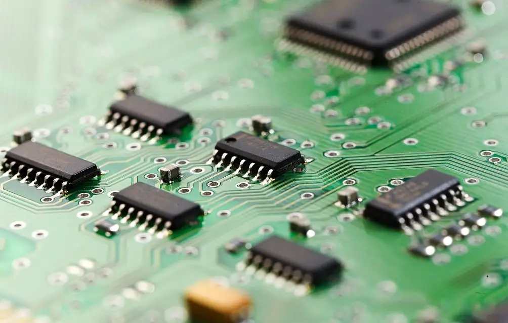
1) SMD components and through-hole components
SMD devices (SMDs) are better at handling RF energy than leaded chips because of their lower inductive reactance and closer placement of components. The lead capacity of through hole components will self oscillate (change from capacity to inductive) at about 80MHz Therefore, noise above 80MHz must be controlled. If through hole components are used in the pipe, many serious problems must be considered for design
2) Basic circuit
Each edge transition transmitted from the microprocessor to another chip is a current pulse that flows to the receiving chip This kind of circuit is ubiquitous in the circuit. Any noise voltage and its accompanying current will return to its source through the impedance path, causing impact The circuit can be signal line and its circuit path, bypass between power supply and ground, crystal oscillator and driver in microprocessor, or return bypass capacitor from power supply voltage regulator The larger the geometric area of the loop, the stronger the radiation. In this case, we can control the shape and impedance of the return path to mitigate noise propagation
3) Differential mode and common mode noise
Differential mode noise is the noise that occurs when a signal travels through the line to the receiving chip and then returns along the return line. There is a voltage difference between the two lines, which is a noise that must be generated when each signal performs its function The electric field strength generated by the noise is proportional to the square of the frequency, and the size of the current and the area of the current loop are inversely proportional to the distance from the observation point to the noise source Therefore, the way to reduce the differential mode radiation is to reduce the working frequency of the circuit, reduce the area of the signal loop or reduce the intensity of the signal current In practice, an effective method is to control the area of the signal loop Common mode noise refers to the noise caused by the common impedance of signal line and return line when the voltage propagates along the signal line and return line at the same time. There is no differential voltage between them Common mode impedance noise is a common noise source in most microprocessor-based systems The electric field strength generated by the noise is proportional to the amplitude of the frequency, and the current and cable length are inversely proportional to the distance from the observation point to the noise source The methods to reduce the common mode radiation are: reduce the impedance of the ground wire, shorten the line length, and use a common mode choke
2. PCB design principles
Since the integration degree and signal frequency of the circuit board are getting higher and higher with the development of electronic technology, electromagnetic interference will inevitably occur Therefore, the following principles should be followed under the following circumstances: designing a PCB to control the electromagnetic interference of the circuit board within a certain range It can meet the design requirements and standards and improve the overall efficiency of the circuit
2.1 Selection of circuit boards
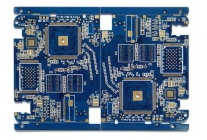
The primary task of PCB design correctly selects the size of PCB if the size is too large, because the connection between components is too long, the impedance value of the line will increase and the anti-interference ability will decrease Dense arrangement of components is not conducive to heat dissipation. If the lines are too thin and dense, it is easy to cause crosstalk Therefore, the circuit board with appropriate size should be selected according to the components required by the system Circuit boards are divided into single-sided, double-sided and multilayer boards The number of circuit board layers depends on the function to be realized by the circuit, noise index, number of signals and network cables, etc A reasonable number of layers can reduce the electromagnetic compatibility problem of the circuit itself The general selection principle is: when the signal frequency is medium low frequency, there are few components, and the wiring density is low or medium, select single side or double side; It is used for high wire density, high integration and multiple components, and uses multi-layer. 3. It is used for high signal frequency, high-speed integrated circuits, and dense components. Select circuit boards with 4 layers or more In the design of Multilayer board, single layer can be used as power layer, signal layer and ground layer The area of signal loop decreases, and the differential mode radiation decreases Therefore, multilayer board can reduce the radiation of circuit board and improve the anti-interference ability
2.2 Layout of circuit board components
After determining the size of the PCB, first determine the position of special components. All components of the circuit shall be arranged in blocks according to the functional unit of the circuit Digital circuit unit, analog circuit unit and power circuit unit shall be separated, and high-frequency circuit unit and low-frequency circuit unit shall also be separated Common circuit board layout principles are as follows
1) The principle of determining the location of special components:
1. The heating element should be placed in a position conducive to heat dissipation, such as PCB, and away from the microprocessor chip;
2. Special high-frequency components should be placed next to each other to shorten the connection between them;
3. Sensitive components should be kept away from noise sources such as clock generators and oscillators;
4. Layout of potentiometer and other adjustable parts, adjustable inductor, variable capacitor, and key switches should conform to the structural requirements of the whole machine and facility adjustment;
5. Components with heavier mass should be fixed with brackets;
6. EMI filter shall be placed close to EMI source


抖音二維碼

Q Q二維碼

微信二維碼
點擊
然后
聯(lián)系
然后
聯(lián)系
電話熱線
13410863085Q Q

微信

- 郵箱