鑫景福致力于滿足“快速服務,零缺陷,輔助研發”PCBA訂購單需求。


PCBA方案設計
Now PCB products and applICations are becoming more and more complex. Integrated processors, memories and other key components have greatly improved in performance specifications. In testing the technical level of PCB design that carries electronIC parts, it is not only necessary to meet the requirements of high density and high efficiency in a SMAll area, but also must be able to have good electrical properties, safety and more stringent use conditions
In recent years, smart phones and tablets have become important product projects that drive the continuous optimization of computer technology. Not only have the products become thinner and lighter, their functions remain unchanged, but also their performance can be upgraded twice or even several tiMES in terms of performance, storage capacity and battery life. In addition to the integration effect of semiconductor technology in 3D IC and high-order heterogeneous packaging technology PCB carrier technology capability upgrade for narrower internal space challenge.
Circuit boards have a great impact on the electronic industry
In fact, long before the appearance of printed circuit boards, most of the components and circuits of electronic products were constructed by directly connecting electronic parts with copper wires to complete the conduction circuit and construct the entire operable electronic product system. However, for electronic circuits constructed in this way, on the one hand, it takes a lot of manpower and effort to make circuits and connect components manually, and the welding of circuits and components is very easy to cause wrong connection, which will cause component or material consumption, increasing the cost of manufacturing and verifying circuits.
The improvement scheme is to use electronic circuit boards to make circuits through metal chEMIcal etching circuits, and drill holes to provide more stable connection and fixation of electronIC components, so as to achieve better circuit connection quality and component fixation effect. At the same time, higher quality circuits can be provided in the production, verification and even after the product is shipped for sales, service and maintenance.
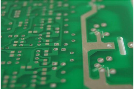
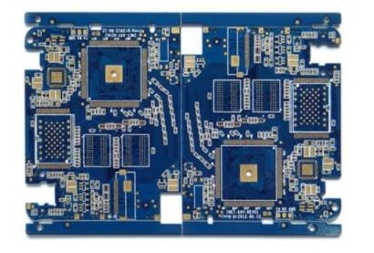
Because the Printed Circuit Board (PCB) plays a key role in carrying a large number of electronic parts and constructing the conductive circuit of components, PCB has also become an important component for the continuous evolution and upgrading of electronic products! The circuit fabrication of PCB is mainly divided into two methods. Basically, PCB itself must have an insulating carrier plate. The carrier plate material determines the strength, insulation effect and basic electrical performance of the PCB itself. The conductive circuit can be constructed by two different fabrication methods, Additive or Subtractive.
PCB soft board? Different advantages of hard boards
The circuit addition method is made by metal electroplating, evaporation plating or conductive material addition of the physical circuit on the substrate; The subtraction rule is to use the printed circuit pattern on the substrate covered with metal conductor layer, and then remove the non printed non circuit block metal through chemical solvent corrosion to form a circuit.
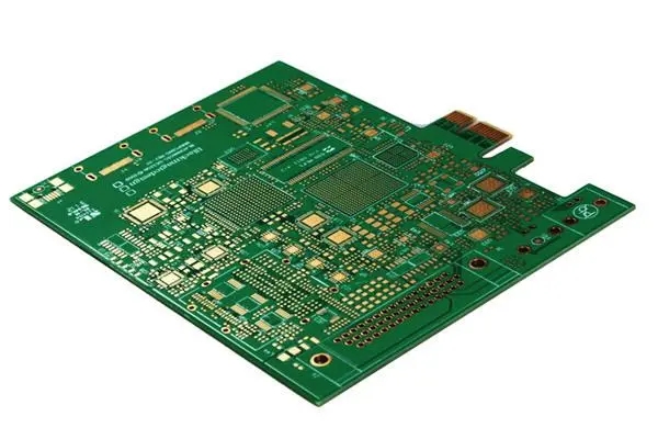
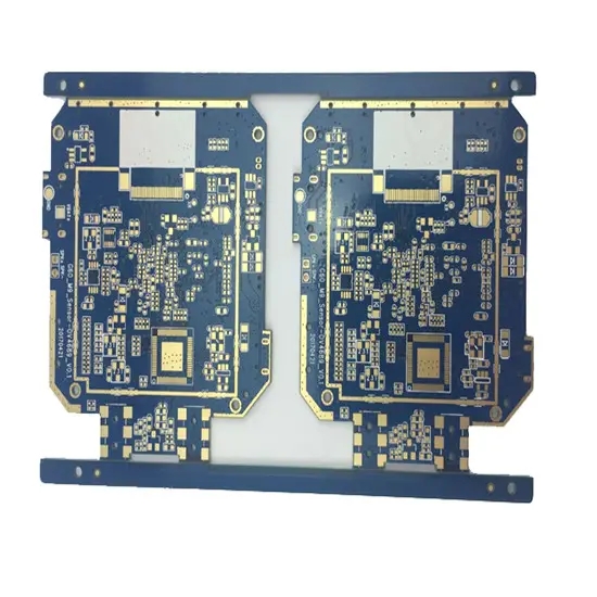
Early substrate materials once beCAMe the bottleneck limiting the application of circuit boards. With the introduction of various machine board materials that give consideration to flexible soft materials, high temperature resistance, thinning and multi-layer stacking applications, such as addition method is often used for processing circuits in high price soft or flexible circuit boards, while subtraction method is used for making circuits in hard circuit boards or multilayer circuit boards in most cases, Soft (flexible) circuit boards and hard circuit boards have different application environments and material characteristics, among which hard circuit boards are much more used, and more sophisticated multilayer boards, high-density Multilayer boards and other advanced products have also been developed, which has become a key core material technology for the design goal of thin, miniaturized or lightweight electronic products.
Test the precision of manufacturing and chemical treatment from single layer to double layer or even multiple layers
Layout design
The conductive layer (circuit) construction of the general substrate can be set on the upper and lower sides of the substrate. The connecting conductive circuit of the upper and lower circuit lines is formed by drilling holes and electroplated through holes in the holes. With the demand of the electronic product industry for high precision and high complexity integrated circuits, the stacking of multiple hard circuit boards, the conductive connection and bonding design between circuit layers, and the construction of a more complex multilayer board structure are also formed.
multilayer circuit boards can effectively SIMplify the size and area of the substrate, especially with highly integrated components of IC technology. Circuit carrier boards can even reduce the spectrum of traditional circuits by several to tens of times, becoming a key design trend for electronic products to actively reduce and optimize.
The integrated design of multilayer boards and high-density circuit boards not only has a much higher in-process technology than conventional circuit boards, but also has a lot more profit than conventional products, but also has more problems. For example, because of the material characteristics of multilayer boards, the temperature generated during the operation of electronic products will also lead to the thermal expansion and cold contraction of the boards. If the connection structure of high-density circuits and the lines connecting layers is fragile, The high operating temperature of the product may also cause open circuit or abnormal conduction of the circuit.
Therefore, although high-density multilayer boards have the advantages of high profits and high material accumulation reduction, the derived testing and verification work will be more complex and demanding. The precision and material temperature changes also need to be optimized through the substrate material to provide high stability and resistance to temperature changes, so that the terminal electronic products can better meet the design requirements.
The choice of metal layer material affects the electrical property of the circuit
In addition to the material characteristics of the substrate, the metal layer placed on the substrate is also the key to the overall performance of the circuit board.
Generally speaking, the material of metal layer is different and the cost gap is huge, which will directly affect the production cost? There are great differences in plug and pull, electrical resistance, thermal conductivity, etc. The actual application is not that the more expensive the material is, the better. Instead, appropriate metal material processing lines must be selected according to the use needs of different metal layers. Common metal layers include copper, tin, lead tin alloy, tin copper alloy, etc. The tin thickness is usually 5~15 μ m. Most lead tin alloys are 5~25 thick μ m。
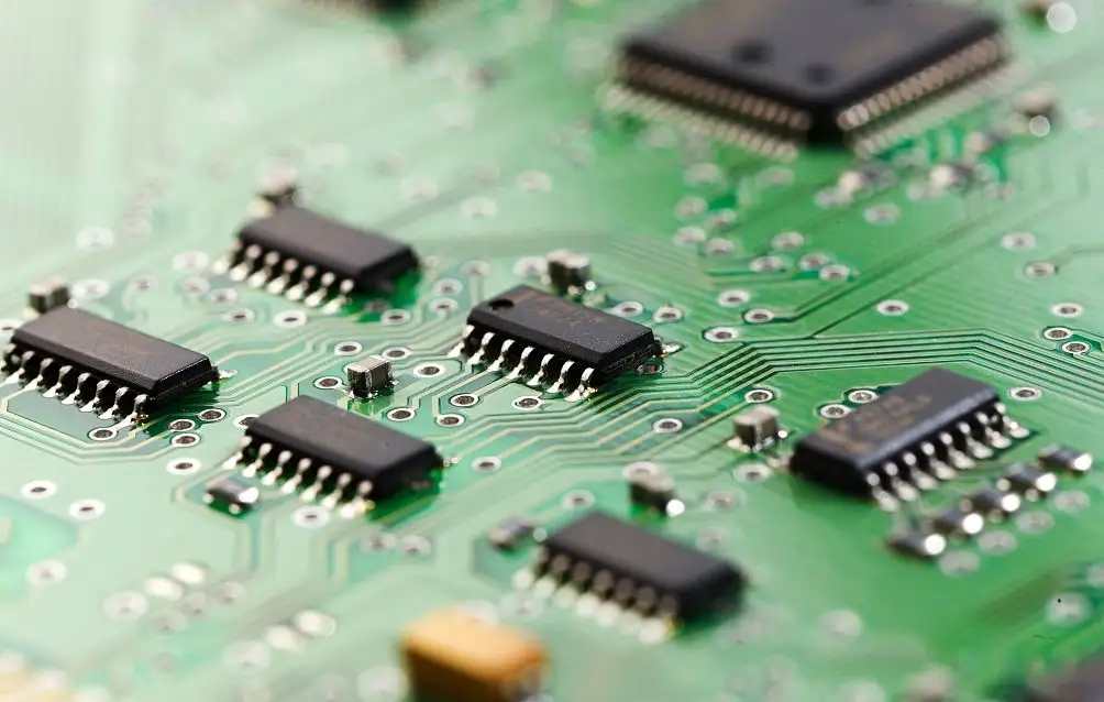
The current circuit board is mainly composed of lines and patterns. Generally, lines and patterns are made together. The insulating plate of the base material itself establishes the insulating electrical properties of each layer (dielectric layer). The carrier plates of each layer form application circuit connections through through holes/via. Generally speaking, the larger through holes are electronic components that need plug-in welding, In addition, the circuit board will also be provided with a non conducting hole for setting and welding the surface adhesive electronic components.
The stability and durability of the circuit board can be improved by matching the board processing at the end of the manufacturing process
If the air is wet, the composite plate itself is also easy to change and deform due to moisture absorption, and the deformation process may lead to breakage or poor contact of the line conductor. In order to increase the life of the board, a layer of epoxy resin is usually added on the non welded surface of the board or the board surface, or it is matched with the reference information such as the name and location of the screen printing element, the version number of the circuit board, and the date of manufacture.
As the copper surface and conductive metal surface on the circuit board are directly in contact with the air, it is very easy to have problems such as plate oxidation, poor tin coating or copper foil falling off due to oxidation deformation. Generally, after the completion of the circuit board, a layer of oxygen resistant protective layer should be added to the metal surface that needs to eat tin, for example, by spraying tin (Hot Air Solder Leveling; HASL), chemical nickel/immersion gold; ENIG) Immersion Ag; Immersion Ag; Immersion Tin or Organic Solderability Preservatives (OSP) are used to protect metal contacts.
As for the verification of circuit board finished products, because the circuit board manufacturing process is complicated, in order to make the products more sophisticated and reduce the number of defective parts, the manufacturing equipment should be regularly maintained and cleaned to maintain stable manufacturing conditions, and the production must also be carried out in a high cleanliness environment to avoid errors in the appearance of finished products.
The plate processing is a multi chemical liquid soaking and processing operation. The equipment must maintain the automatic constant temperature, timing and speed processing of materials. At the same time, the process needs to add chemicals at any time according to the PH value of the liquid materials to maintain the stability of the chemical leaching materials.
In addition to maintaining the product quality by the process standard, the product quality must also rely on the high cleanliness environment to avoid material pollution. For example, the production line can be operated in a dust-free environment, and the liquid photoresist production line must be PCBA processed under the conditions of falling dust filtration and plate dust removal.
Production means paying close attention to the treatment at all stages to maintain consistent quality and reduce production defects
In order to maintain the output quality of the workpieces in the later stage, the quality problems should not be ignored in the process treatment of each PCBA processing section, and the defects in the process and the quality of the final products will also be greatly affected. For each manufacturing process, the first product inspection, the last product inspection, and the intermediate product sampling monitoring need to be implemented to maintain the product PCBA processing quality supervision.
In the drilling process section, pin guage can be used to detect the aperture status and verify the quality of the first article. In the electroplating process, a hand-held hole copper thickness gauge can be used to check the thickness of copper plating, and a chip can be used to check the copper density of the pores and the bonding condition of the inner layer to ensure the quality of the plating holes. After the edge grinding treatment of the plate after copper plating, glass fiber, resin and powder chips are removed, then the abrasive belt machine is used to level the copper surface and remove copper nodules and dents.
At the same time, mass production is assisted by machine vision, supplemented by automatic optical conveyor belt for workpiece detection, while the interlayer alignment of multilayer plates can be detected by X-ray to confirm the accuracy of alignment. In addition, the automatic optical detection can be used with the original circuit drawings for comparison and analysis to prevent the fixed broken line, short circuit or gap of the line of the workpiece.
After pickling, brushing, and micro etching, the bare copper plate in the solder proof process needs to remove the oxide layer and micro copper powder on the copper surface, and increase the roughness of the copper foil itself to improve the adhesion of the ink solder mask, and improve the ability to protect the circuit board. In the printing stage, the ink evenness can be inspected visually. After the circuit board is baked, the thickness of the coated ink must be measured with a film thickness meter.
In the lamination stage, the key is to control the temperature and pressure. In order to achieve the best lamination, the two-part processing can be used to extend the two-part hot pressing time, which can strengthen the hardness, flatness and adhesion of copper foil. In the final verification of the finished PCB, CAM Data can be output, and the automatic fixture software can be used to construct the production program of the biological fixture. The defective workpiece can be selected through the rapid detection of the fixture.


抖音二維碼

Q Q二維碼

微信二維碼
點擊
然后
聯系
然后
聯系
電話熱線
13410863085Q Q

微信

- 郵箱