鑫景福致力于滿足“快速服務,零缺陷,輔助研發”PCBA訂購單需求。


PCBA方案設計
Requirements of PCB proof printing component layout and circuit board design
1、 Discussion on layout and structure design of PCB proofing printed circuit components
For an instrument with excellent performance, in addition to selecting high-quality components and reasonable circuits, the component layout of the printed circuit board and the correct structural design of the electrICal connection direction are the key issues that determine whether the instrument can work reliably. For circuits with the same component and parameter, different results will be produced due to different component layout design and electrical connection direction, and the results may be very different. Therefore, it is necessary to combine the three aspects of how to correctly design the structure of PCB component layout, correctly select the wiring direction and the process structure of the overall instrument. A reasonable process structure can not only eliminate the noise interference caused by improper wiring, but also facilitate the installation, debugging and maintenance in production.
Now we will discuss the above issues. Since there is no strict "definition" and "mode" for excellent "structure", the following discussion is only for reference. The structure of each instrument must adopt corresponding structural design scheme according to specific requirements (electrical performance, overall structure installation, panel layout, etc.), and compare and repeatedly modify several feasible design scheMES.
Wiring structure selection of PCB power supply and ground bus system structure: analog circuit and digital circuit have many SIMilarities and differences in the design and wiring methods of component layout. In analog circuits, due to the existence of amplifiers, the extremely SMAll noise voltage generated by wiring will cause serious distortion of the output signal. In digital circuits, the TTL noise tolerance is 0.4V~0.6V, and the CMOS noise tolerance is 0.3~0.45 times of Vcc. Therefore, digital circuits have strong anti-interference ability.
The reasonable selection of good power and ground bus mode is an important guarantee for the reliable operation of the instrument. A considerable number of interference sources are generated through the power and ground bus, and the noise interference caused by the ground wire is the largest.
2、 Basic principles of PCB proofing pcb design
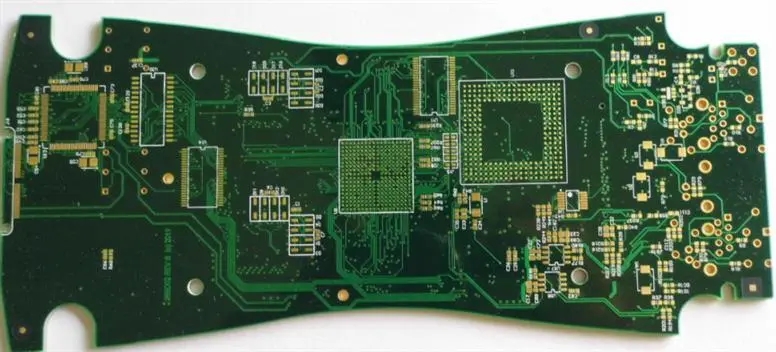
1. The design of the printed circuit board starts from the determination of the size of the board. Because the size of the printed circuit board is limited by the size of the chassis shell, it is appropriate to fit it into the shell. Secondly, the connection mode between the printed circuit board and external components (mainly potentiometers, sockets or other printed circuit boards) should be considered. The printed circuit board and external components are generally connected by plastic wires or metal isolation wires. But sometimes it is also designed as a socket. Namely, when installing a plug-in printed circuit board in the equipment, the contact position that acts as the socket shall be reserved.
For larger components instalLED on the printed circuit board, metal accessories shall be added for fixation to improve the vibration resistance and impact resistance.
2. Basic method of wiring diagram design
First of all, you need to have a complete understanding of the specifications, dimensions, areas, etc. of the selected components and various sockets; Reasonable and careful consideration shall be given to the location arrangement of each component, mainly from the perspective of electromagnetic compatibility, anti-interference, short routing, less crossing, power supply, ground path and decoupling. After the location of each component is determined, it is the online connection of each component. The relevant pins are connected according to the circuit diagram. There are many ways to complete the connection. There are two ways to design the printed circuit diagram: computer aided design and manual design.
The most original is to arrange the layout manually. This is rather laborious, and it often needs to be repeated several times before it can be finally completed. This can also be done when there is no other drawing equipment. This manual layout method is also very helpful for designers who are just learning the printed board drawing. There are many kinds of computer aided drawing software with different functions, but generally speaking, it is convenient to draw and modify, and can be saved, stored and printed.
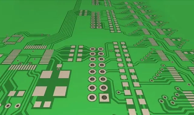
Next, determine the required size of the PCB, and preliminarily determine the position of each component according to the schematic diagram, and then continuously adjust to make the layout more reasonable. The wiring arrangement between components in the PCB is as follows:
(1) Cross circuits are not allowed in printed circuits. Lines that may cross can be solved by "drilling" or "winding". That is to say, let a lead "drill" through the gap at the foot of other resistors, capacitors, and transistors, or "wind" through one end of a lead that may cross. Under special circumstances, how to make the circuit very complex? In order to simplify the design, it is also allowed to use a wire jumper to solve the cross circuit problem.
(2) Resistance, diode, tubular capacitor and other components can be installed in "vertical" and "horizontal" modes. Vertical refers to the installation and welding of components perpendicular to the circuit board, which has the advantage of saving space. Horizontal refers to the installation and welding of components parallel to and close to the circuit board, which has the advantage of good mechanical strength for component installation. For these two different mounting components, the component hole spacing on the printed circuit board is different.
(3) The grounding point of the circuit at the same level shall be as close as possible, and the power filter capacitor of the circuit at this level shall also be connected to the grounding point at this level. In particular, the ground points of the base and EMItter of the current transistor cannot be too far away, otherwise the copper foil between the two ground points will be too long, which will cause interference and self excitation. The circuit using this "one point grounding method" will work more stably and is not easy to self excitation.
(4) The general grounding wire must be arranged in the order from weak current to strong current in a high frequency medium frequency low frequency level. It is not allowed to randomly turn over and over. It is better to have a long connection between levels, but also to comply with this provision. In particular, the grounding wire arrangement of frequency converter head, regeneration head and frequency converter head is more strict. If it is improper, self excitation will occur and it will not work.
High frequency circuits such as FM head often use a large area of enclosed ground wire to ensure a good shielding effect.
(5) Strong current leads (common ground wire, power amplifier power lead, etc.) should be as wide as possible to reduce wiring resistance and its voltage drop, and reduce self excitation caused by parasitic coupling.
(6) The route with high impedance shall be as short as possible, and the route with low impedance may be longer, because the route with high impedance is easy to whistle and absorb signals, causing circuit instability. The power line, ground wire, base wire without feedback component, emitter wire, etc. are all low impedance wires. The base wire of the emitter follower and the ground wire of the two audio channels of the radio recorder must be separated and formed into one circuit respectively until the end of the function. If the two ground wires are connected, it is very easy to produce crosstalk and reduce the separation. PCB manufacturers, PCB designers, and PCBA processors will explain the requirements for the layout of pcb proofing printing components and PCB drawing design.


抖音二維碼

Q Q二維碼

微信二維碼
點擊
然后
聯系
然后
聯系
電話熱線
13410863085Q Q

微信

- 郵箱