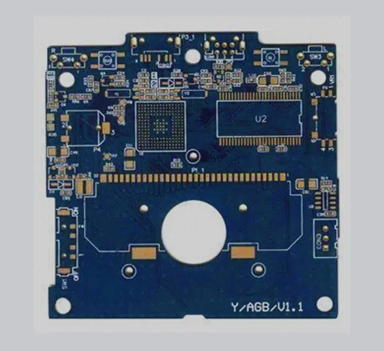
鑫景福致力于滿足“快速服務,零缺陷,輔助研發”PCBA訂購單需求。


PCBA方案設計
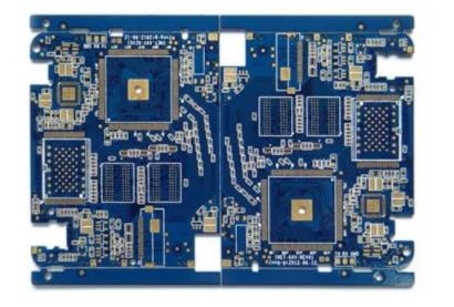
The SMAll editor of Pcb factory talks about the second paragraph of high-speed PCB design rules for you in detail
24. Crystals, crystal oscillators, relays, switching power supplies and other strong radiation devICes shall be at least 1000 mils away from the board interface connector.
Cause: The interference will radiate outward directly or couple the current on the outgoing cable to radiate outward.
25. Sensitive circuits or devices (such as reset circuits, WATCHDOG circuits, etc.) shall be at least 1000 mils away from the edges of boards, especially the edges of board interfaces.
Cause: Places like the board interface are most susceptible to external interference (such as static electricity) coupling, while sensitive circuits such as reset circuit and watchdog circuit are very likely to cause system misoperation.
26. Each filter capacitor for IC filtering shall be placed as close as possible to the power supply pin of the chip.
Cause: The closer the capacitor is to the pin, the smaller the area of the high-frequency circuit, and thus the smaller the radiation.
27. The matching resistor in series at the starting end shall be placed close to its signal output end.
Cause: The design purpose of the series matching resistance at the beginning is to make the sum of the output impedance of the chip output end and the impedance of the series resistance equal to the characteristic impedance of the wiring. The matching resistance is placed at the end, which cannot meet the above equation.
28. PCB wiring shall not have right angle or acute angle wiring.
Cause: The right angle wiring leads to discontinuous impedance, leading to signal transmission, resulting in ringing or overshoot, forming strong EMI radiation.
29. Avoid layer setting of adjacent wiring layers as much as possible. If it cannot be avoided, try to make the routing in the two wiring layers perpendicular to each other or the parallel routing length less than 1000 mils.
Cause: reduce crosstalk between parallel lines.
30. If the board has an internal signal routing layer, the clock and other key signal lines are laid in the inner layer (the routing layer is preferred).
Cause: The key signals can be shielded by laying them on the internal wiring layer.
31. It is recommended to wrap the ground wire on both sides of the clock wire, and the grounding via should be punched every 3000mil.
Cause: ensure that the potential of each point on the grounding wire is equal.
32. Clock, bus, RF cable and other key signal wiring: other parallel wiring on the same layer shall meet the 3W principle.
Cause: Avoid crosstalk between signals.
33. The bonding pads of surface mounted fuses, magnetic beads, inductors and tantalum capacitors used for power supply with current ≥ 1A shall be connected to the plane layer through at least two vias.
Cause: reduce the equivalent impedance of vias.
34. The differential signal lines shall be laid in the same layer, of equal length and in parallel, with the same impedance and no other lines between the differential lines.
Reason: ensure the common mode impedance of differential line pair is equal, and improve its anti-interference capability.
35. The key signal routing must not cross the partition area (including the reference plane gap caused by vias and pads).
Cause: Wiring across the partition will lead to an increase in the area of the signal loop.
36. When it is unavoidable for the signal line to split the ground across its return plane, it is recommended to use bridge capacitance near the signal cross split, and the capacitance value is 1nF.
Cause: When the signal is split across, the circuit area is often increased. The bridge grounding method is used to set the signal circuit for it manually
37. No other irrelevant signals shall be routed below the filter (filter circuit) on the board.
Cause: Distributed capacitance will weaken the filtering effect of the filter.
38. The input and output signal lines of the filter (filter circuit) shall not be parallel or crossed.
Cause: Avoid direct noise coupling before and after filtering.
39. The distance from the key signal line to the edge of the reference plane is ≥ 3H (H is the height of the line from the reference plane).
Cause: inhibit the edge radiation effect.
40. For metal shell grounding element, the top layer of its projection area shall be paved with grounding copper sheet.
Cause: The distributed capacitance between the metal shell and the grounding copper sheet is used to restrain its external radiation and improve its immunity.
41. In the single layer board or double layer board, attention should be paid to the "loop area minimization" design when wiring.
Cause: The smaller the loop area is, the smaller the external radiation of the loop is, and the stronger the anti-interference ability is.
42. When the signal lines (especially the key signal lines) change layers, they should be designed to pass holes near the layer change holes.
Cause: It can reduce the area of signal loop.
43. Clock line, bus, radio frequency line, etc.: The strong radiation signal line is far away from the outgoing signal line of the interface.
Cause: The interference on the strong radiation signal line shall not be coupLED to the outgoing signal line and radiate outward.
44. Sensitive signal lines, such as reset signal lines, chip selection signal lines, system control signals, are far away from interface outgoing signal lines.
Cause: External interference is often brought in by the outgoing signal line of the interface, which will lead to system misoperation when coupled to the sensitive signal line.
45. In the single panel and double-sided panel, the routing of the filter capacitor shall be filtered by the filter capacitor first, and then to the device pin.
Cause: The power supply voltage is filtered before supplying power to the IC, and the noise fed back to the power supply by the IC is filtered by the capacitor.
46. In the single panel or double sided panel, if the power line runs very long, the decoupling capacitance should be added to the ground every 3000mil, and the capacitance value is 10uF+1000pF.
Cause: Filter the high-frequency noise on the power line.
47. The grounding wire and power supply wire of the filter capacitor should be as thick and short as possible.
Cause: The equivalent series inductance will reduce the resonant frequency of the capacitor and weaken its high-frequency filtering effect.
PCB manufacturers, PCB designers and PCBA manufacturers will explain the second paragraph of high-speed PCB design rules to you.


抖音二維碼

Q Q二維碼

微信二維碼
點擊
然后
聯系
然后
聯系
電話熱線
13410863085Q Q

微信

- 郵箱