鑫景福致力于滿足“快速服務,零缺陷,輔助研發”PCBA訂購單需求。


PCBA方案設計
Clever Skills of PCB Layout and Treatment of Process Defects
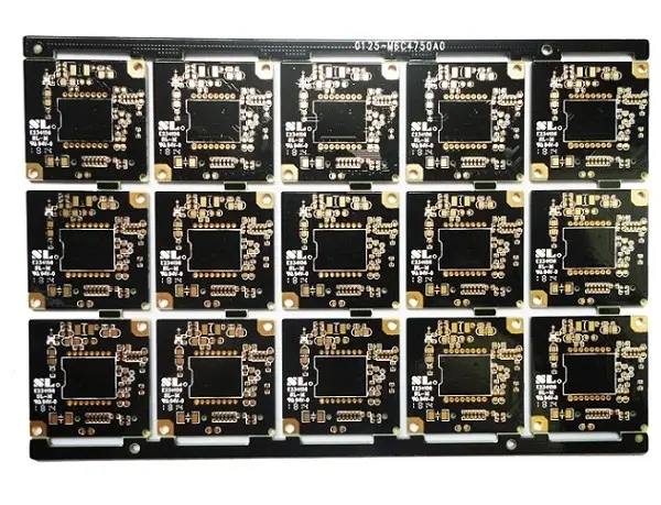
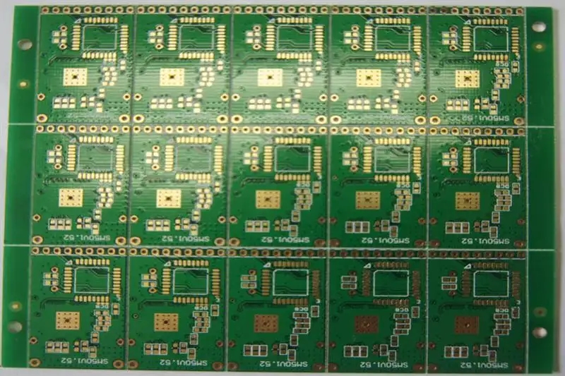
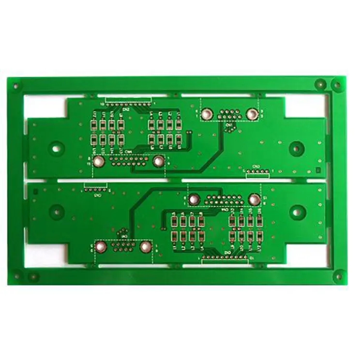
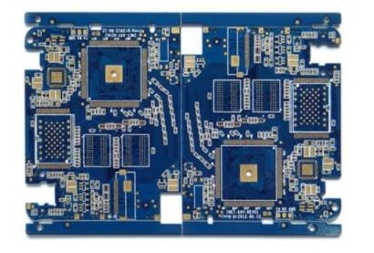
PCB (edcircuit board), Chinese name is printed circuit board, also known as printed circuit board, printed circuit board, is an important electronIC component, is the support of electronIC components, and is the electrical connection provider of electronic components. Because it is made by electronic printing, it is calLED "printed" circuit board.
As PCB size requirements become SMAller and smaller, device density requirements become higher and higher, and PCB design becoMES more and more difficult. How to achieve high PCB routing rate and shorten the design time? Here the author talks about the design skills of PCB planning, layout and routing.
Before wiring, the design should be carefully analyzed and the tool software should be carefully set, which will make the design more consistent with the requirements.
1. Determine the number of layers of PCB
The size of the circuit board and the number of wiring layers need to be determined at the initial stage of design. The number of wiring layers and the way of stacking (STack up) will directly affect the wiring and impedance of the printed wire. The size of the board is helpful to determine the stacking mode and the width of the printed line to achieve the desired design effect. At present, the cost difference between multilayer boards is very small, so it is better to use more circuit layers and make copper coating evenly distributed at the beginning of design.
2. Design rules and limitations
To successfully complete the routing task, the routing tool needs to work under the correct rules and restrictions. To classify all signal lines with special requirements, each signal class should have priority. The higher the priority, the stricter the rules. The rules involve the width of printed wire, the maximum number of vias, parallelism, the interaction between signal wires, and layer restrictions. These rules have a great impact on the performance of wiring tools.
Careful consideration of design requirements is an important step for successful cabling.
In the process of optimal assembly, the design for manufacturability (DFM) rules will limit the component layout. If the assembly department allows the components to move, the circuit can be properly optimized to facilitate automatic wiring. The rules and constraints defined affect the layout design. The automatic routing tool only considers one signal at a time. By setting the constraints of routing and the layers that can be used to route signal lines, the routing tool can complete the routing as envisaged by the designer.
For example, for power cord layout:
In PCB layout, the power decoupling circuit should be designed near each related circuit, not placed in the power supply part, otherwise it will not only affect the bypass effect, but also flow pulsating current on the power line and ground wire, causing interference;
For the internal power supply direction of the circuit, power shall be supplied from the last stage to the next stage, and the power filter capacitor of this part shall be arranged near the last stage;
For some main current channels, such as disconnecting or measuring the current during commissioning and testing, the current gap shall be arranged on the printed wire during layout.
In addition, it should be noted that the regulated power supply should be arranged on a separate printed board as far as possible. When the power supply and circuit share a printed board, in the layout, it should be avoided to mix the regulated power supply and circuit components or make the power supply and circuit share a ground wire.
Because this kind of wiring is not only easy to cause interference, but also cannot disconnect the load during maintenance, so only part of the printed wire can be cut, thus damaging the printed board.
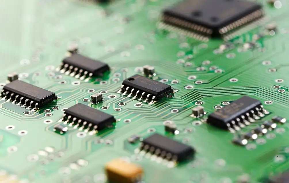
4. Fan out design
At the fan out design stage, each pin of the surface mount device should have at least one via, so that when more connections are needed, the circuit board can carry out internal connection, online testing and circuit reprocessing.
In order to maximize the efficiency of the automatic routing tool, it is necessary to use the largest via size and printed wire as much as possible, and it is ideal to set the spacing at 50mil. Use the type of vias that maximize the number of routing diameters. After careful consideration and prediction, the design of circuit online test can be carried out at the initial stage of design and realized at the later stage of production process.
The type of via fan out is determined according to the wiring path and circuit online test. The power and grounding will also affect the wiring and fan out design.
PCB manufacturers, PCB designers and PCBA processors will explain the ingenious skills of PCB layout and the treatment of process defects.


抖音二維碼

Q Q二維碼

微信二維碼
點擊
然后
聯系
然后
聯系
電話熱線
13410863085Q Q

微信

- 郵箱