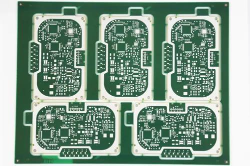
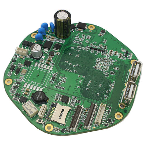
鑫景福致力于滿足“快速服務,零缺陷,輔助研發”PCBA訂購單需求。


PCBA方案設計
ElectronIC manufacturers: six good habits to make your PCB design better
PCB layout engineers route thousands of wires to boards every day, and repeat the work of pulling wires for various packages. Maybe many people will find it very boring. It seems that the software operation porter, in fact, the designer should make a choice between various design rules in the process, taking into account performance, cost, process and other aspects, and also pay attention to the reasonable and orderly layout of the board. It is not as SIMple as it seems, and requires more wisdom. Good working habits will benefit you greatly, making your design more reasonable, production easier and performance better. Here are six good habits that have benefited you a lot.
(1) Details determine success or failure
PCB design is a meticulous work, which requires care and patience. The mistakes that novice designers often make at the beginning are some details. The device pin is wrong, the device package is used incorrectly, the pin sequence is reversed, etc. Some can be solved by flying wire, and some may turn a board directly into a waste product. Check the package more than once when drawing the package, and compare the package print with the actual device before dropping the board. Check more than once is not an obsessive-compulsive disorder, but to avoid these easy to make low-level errors as much as possible. Otherwise, no matter how good-looking the board is, it will be far from excellent if it is covered with flying lines.
(2) Learn to set rules
In fact, not only advanced PCB design software needs to set routing rules, but also some simple and easy-to-use PCB tools can set rules. After all, the human brain is not a machine, so there will inevitably be negligence and mistakes. So we set some problems that are easy to ignore into the rules, and let the computer help us to check, so as to avoid making some low-level mistakes. In addition, perfect rule settings can better standardize the following work. The more complicated the size of the board is, the more important the rules are. Now many EDA tools have the automatic wiring function. If the rules are set in sufficient detail, let the tool help you to design. Wouldn't it be more comfortable for you to have a cup of coffee?
(3) The more you think about others, the less you work
When designing PCB, try to consider the needs of some end users as much as possible. For example, if you are designing a development board, you should consider placing more screen information when designing a PCB, so that it will be more convenient to use it without having to search for schematic diagrams or find support from designers back and forth. If the design is a mass production product, more consideration should be given to the problems encountered on the production line. The same type of devices should be in the same direction as far as possible, whether the device spacing is appropriate, and the process edge width of the board. The earlier these problems are considered, the less they will affect the later design. It can also reduce the workload and the number of board changes. It seems that it takes more time to start the design, which actually reduces the subsequent workload. If the board subspace signal allows, try to place more test points to improve the testability of the board, so as to save more time and provide more ideas for finding problems in the subsequent debugging phase.
(4) Draw the schematic diagram
Many engineers think that layout is more important. The schematic diagram is used to generate a net list for PCB inspection. In fact, the schematic diagram will play a greater role in the subsequent circuit debugging. Whether it is to find problems or communicate with colleagues, or the schematic diagram is more intuitive and convenient. In addition, develop the habit of MARKing in the schematic diagram, and mark the problems that should be noticed in the layout of each part of the circuit on the schematic diagram, which is a good rEMInder for yourself or others. Hierarchical schematic diagrams divide circuits of different functions and modules into different pages, so that the workload can be significantly reduced both in reading diagrams and in future reuse. Using a mature design is always less risky than designing a new circuit. Every time you see all the circuits on a piece of paper, a dense piece of devices, your head can be a big circle.
(5) Make a good circuit layout
The anxious engineer finished drawing the schematic diagram, and after importing the net list into the PCB, he could not wait to put the components in place and start pulling lines. In fact, a good PCB layout can make the pulling work behind you easier and make your PCB work better. Each board will have a signal path, and PCB layout should also follow this signal path as far as possible, so that signals can be transmitted smoothly on the board. People do not like to walk in a maze, so do signals. If the schematic diagram is designed according to the module, PCB can also be used. The board can be divided into several areas according to different functional modules. Separate analog from digital, separate power supply from signal, separate heating devices from sensitive devices, keep larger devices away from the edge of the board, pay attention to the shielding of RF signals, etc... Spend an extra minute to optimize the PCB layout, and you can save more time when pulling wires.
(6) Try to simulate
Simulation is often something that PCB design engineers are unwilling to touch. Maybe someone will say that even if I simulate, there will still be differences between the actual PCB and the simulation results. Why do I waste time doing simulation? I don't simulate the boards that work well? I am helpless to this idea. There is no problem with one or two designs, which does not mean that there will be no problems in the future. Although the simulation results are different from the actual results, the simulation can show the correct trend, and we can make our own judgments according to the trend. At the beginning, there may be difficulties. It is normal to be confused about the simulation model of simulation parameters. As long as you start, work slowly and accumulate slowly, you will realize the importance of simulation. Before the board is completed, determine the position where problems are likely to occur in advance, and solve it in advance to avoid problems. If more simulation is done, the root cause of the problem will be found out and it will also be helpful to improve your design ability.
In actual work, if you can pay attention to the problems mentioned above and develop a good working habit, you will be able to complete more and better designs with the gradual improvement of your personal ability. PCB manufacturers, PCB designers and PCBA manufacturers explain six good habits to make your PCB design better.


抖音二維碼

Q Q二維碼

微信二維碼
點擊
然后
聯系
然后
聯系
電話熱線
13410863085Q Q

微信

- 郵箱