鑫景福致力于滿足“快速服務(wù),零缺陷,輔助研發(fā)”PCBA訂購單需求。


PCBA方案設(shè)計(jì)
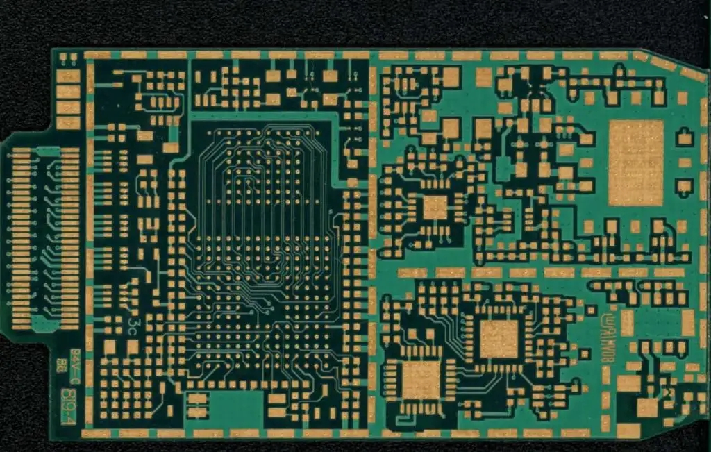
Anti interference design of High Frequency Circuit Board
With the development of communICation technology, wireless high-frequency circuit technology is used more and more widely. The performance index of high-frequency circuit directly affects the quality of the whole product. The layout and wiring of components can maximize the performance index of the circuit and achieve the anti-interference design purpose.
Because the surface mount generally uses infrared furnace thermal flow welding to realize the welding of components, the Layout of components affects the quality of solder joints, and then affects the yield of products.
In addition to the layout of common PCB design, how to reduce the mutual interference between various parts of the high-frequency circuit, how to reduce the interference of the circuit itself to other circuits and the anti-interference ability of the circuit itself are also considered when designing the high-frequency circuit PCB.
The effect of high frequency circuit depends not only on the performance index of the High Frequency Circuit Board itself, but also on the interaction between the high frequency circuit board and the CPU processing board. Therefore, the reasonable layout in PCB design. The general principle of layout is that components should be arranged in the same direction as far as possible, and poor soldering can be reduced or even avoided by selecting the direction of PCB entering the tin melting system;
Details in layout:
1) First, determine the position of the interface components with other PCB boards or systems on the PCB board, and pay attention to the coordination between the interface components (the direction of Canadian components, etc.);
2) Because the size of handheld devices is very SMAll, and the arrangement of components is very compact, for larger components, priority must be given to determine the corresponding location and consider the coordination between them;
3) Carefully analyze the circuit structure, process the circuit in blocks (add high-frequency amplification circuit, frequency mixing circuit, demodulation circuit, etc.), try to separate the strong current signal from the weak current signal, separate the digital signal circuit from the analog signal circuit, and try to arrange the circuits that complete the same function within a certain range, so as to reduce the signal loop area; The filter network of each part of the circuit must be connected nearby, which can not only reduce the radiation height, but also reduce the probability of being interfered, and improve the anti-interference ability of the circuit;
4) The unit circuits are grouped according to their sensitivity to electromagnetic compatibility in use.
2. Wiring
After the layout of components is basically completed, the wiring can be started. The basic principle of wiring is: if the assembly density permits, low-density wiring design shall be selected as far as possible, and the signal wiring shall be as thick and thin as possible, which is conducive to impedance matching.
In the design of high-frequency Circuit PCB, the direction, width and line spacing of signal lines shall be comprehensively considered, and the wiring shall be reasonable. During wiring, all wires shall be about 2 mm away from the frame of the PCB board, so as to avoid wire breakage or potential wire breakage during PCB manufacturing.
The power line shall be as wide as possible to reduce the loop resistance, and the direction of power line and ground wire shall be consistent with the direction of data transmission to improve the anti-interference capability; The signal wires shall be as short as possible and the number of vias shall be minimized; The shorter the connection between components, the better, to reduce the distribution parameters and mutual electromagnetic interference; The incompatible signal lines shall be kept away from each other as far as possible, and parallel routing shall be avoided as far as possible, while the signal lines on both sides shall be perpendicular to each other; When wiring, 135 ° angle should be used where corners are needed to avoid turning right angles.


抖音二維碼

Q Q二維碼

微信二維碼
點(diǎn)擊
然后
聯(lián)系
然后
聯(lián)系
電話熱線
13410863085Q Q

微信

- 郵箱