鑫景福致力于滿足“快速服務(wù),零缺陷,輔助研發(fā)”PCBA訂購單需求。


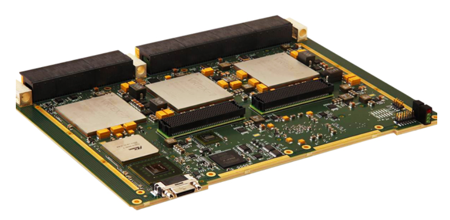
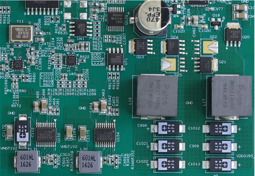
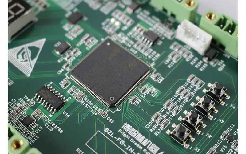
PCBA加工
In the PCB electronic industry welding process, more and more circuit board welding manufacturers begin to focus on selective welding. Selective welding can complete all the solder joints at the same time, minimizing the production cost. At the same time, it overcoMES the impact of reflow welding on temperature sensitive components. Selective welding can also be compatible with lead-free welding in the future. These advantages make selective welding more and more widely used.

Process characteristICs of selective welding
The process characteristics of selective welding can be understood by comparing with wave soldering. The most obvious difference between the two is that the lower part of PCB in wave soldering is completely immersed in liquid solder, while in selective soldering, only some specific areas are in contact with solder wave. Because PCB itself is a bad heat conduction medium, it will not heat and melt the solder joints of adjacent components and pcb areas during welding. Flux must also be pre coated before welding. Compared with wave soldering, flux is only applied to the lower part of PCB to be welded, not the whole PCB. In addition, selective welding is only applicable to the welding of plug-in components. Selective welding is a new method, and a thorough understanding of the selective welding process and equipment is necessary for successful welding.
Process of selective PCB welding
Typical selective welding processes include flux spraying, PCB preheating, DIP welding and drag welding.
Flux coating process
Flux coating process plays an important role in selective welding. During welding heating and at the end of welding, the flux shall have sufficient activity to prevent bridging and oxidation of pcb. Flux spraying: the x/y manipulator carries the pcb over the flux nozzle, and the flux is sprayed to the position where the pcb is to be welded. Flux has a variety of ways, including single nozzle spray, micropore spray, and synchronous multi-point/pattern spray. The most important thing for microwave peak selection welding after reflow welding sequence is accurate spraying of flux. The micro hole spray type will never contaminate the area outside the solder joint. The minimum flux spot pattern diameter of micro spot spraying is greater than 2mm, so the position accuracy of the flux sprayed and deposited on the pcb is ± 0.5mm, which can ensure that the flux always covers the welded part. The tolerance of the amount of sprayed flux is provided by the supplier. The technical specification should specify the amount of flux used, and it is generally recommended that the 100% safety tolerance range.
Preheating process
The main purpose of preheating in the selective welding process is not to reduce the thermal stress, but to remove the solvent pre drying flux, so that the flux has the correct viscosity before entering the solder wavefront. During welding, the influence of the heat carried by preheating on the welding quality is not a key factor. pcb material thickness, device package specification and flux type determine the preheating temperature setting.
In selective welding, there are different theoretical explanations for preheating: some process engineers believe that pcb should be preheated before flux spraying; Another view is that welding is carried out directly without preheating. Users can arrange the process flow of selective welding according to specific conditions.
Selective welding process
There are two different processes for selective welding: drag welding and immersion welding.
The selective drag welding process is completed on a single SMAll tip solder wave. Drag welding process is suitable for welding in very close space on pcb board.
For example, for individual solder joints or pins, a single row of pins can be used for drag welding. Pcb moves on the solder wave of the welding nozzle at different speeds and angles to achieve the best welding quality. To ensure the stability of the welding process, the inner diameter of the welding nozzle is less than 6mm. After the flow direction of solder solution is determined, the welding nozzle is instalLED and optimized in different directions for different welding needs. The manipulator can approach the solder wave from different directions, i.e. 0 °~12 ° at different angles, so users can weld various devices on electronIC components. For most devices, it is recommended that the tilt angle be 10 °.
Compared with the dip welding process, the heat conversion efficiency of the drag welding process is better than that of the dip welding process due to the movement of solder solution and pcb board. However, the heat needed to form the weld connection is transferred by the solder wave, but the quality of the solder wave of a single nozzle is small. Only the temperature of the solder wave is relatively high can it meet the requirements of the drag welding process.
For example, the soldering temperature is 275 ℃~300 ℃, and the pulling speed is generally acceptable, which is 10 mm/s~25 mm/s. Nitrogen is supplied in the welding area to prevent solder wave oxidation. Solder wave eliminates oxidation, so that the drag welding process can avoid bridging defects. This advantage increases the stability and reliability of the drag welding process.
The machine has the characteristics of high precision and high flexibility. The system designed with module structure can be customized completely according to the special Production requirements of customers, and can be upgraded to meet the needs of future production development. The movement radius of the manipulator can cover the flux nozzle, preheating and solder nozzle, so the same equipment can complete different welding processes. The unique synchronous manufacturing process of the machine can greatly shorten the single board manufacturing process cycle. The ability of the manipulator makes this selective welding have the characteristics of high precision and high quality welding. Firstly, the highly stable precise positioning capability of the manipulator (± 0.05mm) ensures the repetition and consistency of the parameter height of each plate production; Secondly, the 5-dimensional motion of the manipulator enables the pcb to contact the tin surface at any optimal angle and orientation to obtain the best welding quality. The tin wave height measuring needle installed on the manipulator splint device is made of titanium alloy. Under the program control, the tin wave height can be measured regularly. The tin wave height can be controlled by adjusting the speed of the tin pump to ensure process stability.
DeSPIte these advantages, PCB single nozzle solder wave drag welding process also has shortcomings: PCB welding time is the longest among the three processes of flux spraying, preheating and welding. And because the solder joints are dragged one by one, the welding time will increase significantly with the increase of the number of solder joints, and the welding efficiency cannot be compared with the traditional PCB wave soldering process. However, the situation is changing. The design of multiple welding nozzles can maximize the output. For example, the use of double welding nozzles can double the output, and the flux can also be designed as double nozzles.

抖音二維碼

Q Q二維碼

微信二維碼
點(diǎn)擊
然后
聯(lián)系
然后
聯(lián)系
電話熱線
13410863085Q Q

微信

- 郵箱