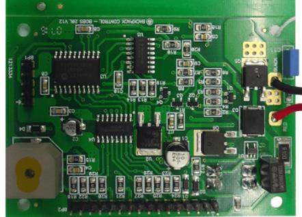
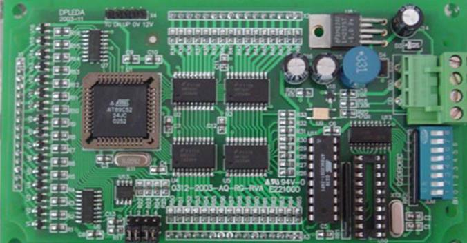
鑫景福致力于滿足“快速服務,零缺陷,輔助研發”PCBA訂購單需求。


PCBA加工
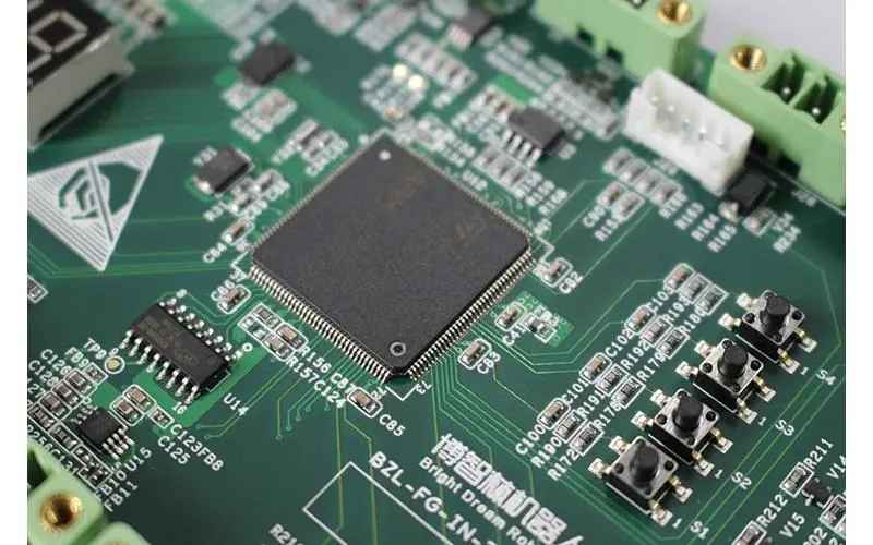
Six Common Integrated Circuit Packages
1 SO package
Use this SMAll package when there are fewer wires for most small scale integrated circuits There are several types of SO packages If the chip width is less than 0.15 inch, and the number of electrIC pins is relatively small (usually between 8 and 40 pins), it is calLED SOP package; The chip width is greater than 0.25 inch, and the number of electrode pins is greater than 44 This kind of chip is commonly used in random access memory (RAM); The chip width is more than 0.6 inch, and the number of electrode pins exceeds 44. It is called SOW package, this kind of chip is commonly used in programmable memory (E2PROM) Some SOP packages use small or thin packages, which are called SSOP packages and TSOP packages, respectively Most SO package pins use wing electrodes, and some memories use J-shaped electrodes (called SOJ), which is conducive to expanding the storage capacity on the socket The lead spacing of SO package is 1.27mm, 1.0mm, 0.8mm, 0.65mm and 0.5mm
2. QFP package
QFP (Quad Flat Package) is a quad pin flat package, which is one of the main packaging forms of surface mount integrated circuits. The pin is drawn into the shape of the wing (L) from four sides. There are three kinds of substrates: ceramics, metals and plastics. In terms of quantity, plastic packaging accounts for the vast majority. When the information is not clearly stated, it is plastic QFP in most cases. Plastic QFP is the most popular multi pin LSI package. It is not only used in digital logic LSI such as microprocessors and gate arrays, but also used in analog LSI such as VTR signal processing and audio signal processing. There are various specifications of pin center distance, such as 1.0mm, 0.8mm, 0.65mm, 0.5mm, 0.4mm, 0.3mm, etc. The minimum pin spacing is 0.3mm and the maximum pin spacing is 1.27mm. The maximum number of pins in 0.65mm center distance specification is 304.
In order to prevent pin deformation, several improved QFP varieties have emerged. For example, BQFP with resin cushion pads (corner lugs) on the four corners of the package has protrusions on the four corners of the package to prevent the pin from bending and deformation during transportation or operation.
3. PLCC package

PLCC is a lead plastIC chip carrier package for integrated circuits. Its electrode pin hooks inward, called hook shaped (J-shaped) electrode. The number of electrode pins is 16 to 84 and the spacing is 1.27 mm. Most integrated circuits packaged by PLCC are programmable memory. The chip can be installed on a special socket and can be easily removed to rewrite data; In order to reduce the cost of the socket, PLCC chips can also be directly welded to the circuit board, but manual welding is more difficult. PLCC is square and rectangular in appearance. The square is called JEDEC MO-047, with 20~124 pins; The rectangle is called JEDEC MO-052 and has 18 to 32 pins.
4. LCCC package
LCCC is a kind of packaging, which is packaged by ceramic chip carrier in SMD integrated circuit; The chip is packaged on a ceramic carrier in square and rectangular shapes The lead-free electrode solder end is set at the four sides of the package bottom The square numbers of electrodes are 16, 20, 24, 28, 44, 52, 68, 84, 100, 124, and 156, and the rectangles are 18, 22, 28, and 32, respectively There are two pilot pitches: 1.0mm and 1.27mm
LCCC outgoing terminals are characterized by a castle shaped metallized slot on the side of the ceramic shell, which is connected with the gold plated electrode at the bottom of the shell, providing a short MESsage signal path, low inductance and capacitance loss, and can be used for high-frequency working conditions such as microprocessor units, gate arrays and memories.
The chip of LCCC integrated circuit is fully sealed, with high reliability but high price. It is mainly used for military products. It must be considered whether the thermal expansion coefficient between the device and the circuit board is consistent.
5. PQFN package
PQFN is a square or rectangular lead-free package. There is a large exposed pad at the bottom center of the package, which improves the heat dissipation efficiency. A conductive pad used for electrical connection around the package around a large pad. Because PQFN package does not have SOP, QFP and other wing shaped pins, the conductive path between the internal pin and the bonding pad is short, and the self inductance and wiring resistance in the package are very low, which can provide good power efficiency. Due to its good power and thermal efficiency, small size and low quality, PQFN has become an ideal choice for many new applications. PQFN is very suitable for high-density products, such as mobile phones, digital CAMeras, PDAs, DVs, smart cards and other portable Electronic devices.
6. BGA package
BGA package is a ball grid array package. It changes the J-shaped or wing shaped electrode pin of the original device PccQFP package to a spherical pin, and changes the "single wire" sequence of electrodes from the periphery of the device body to the "complete" sequence at the bottom of the body. Lay out a "flat" grid array. In this way, the pin spacing can be emptied and the number of pins can be increased. The solder ball array can be completely or partially distributed on the bottom surface of the device.
The BGA method can significantly reduce the package surface area of the chip: Suppose the LSI has 400 input/output electrode pins, and the same pin spacing is 1.27 mm, then the square QFP chip has 100 pins on each side, and one side is very long. At least 127 mm, and the surface area of the chip must be 160 cm2; The electrode pins of the square BGA chip are uniformly arranged into 20 under the chip × 20 rows, the side length is only 25.4mm, and the surface area of the chip is less than 7cm2. It can be seen that for LSI with the same function, the size of BGA package is much smaller than QFP, which is conducive to improving the assembly density on PCB.
From the perspective of assembly and welding, the installation tolerance of BGA chip is 0.3mm, which is far lower than the requirement of 0.08mm for QFP chip. This makes the installation reliability of BGA chip significantly improved and the process error rate greatly reduced. The general multifunctional mounting machine and reflow soldering equipment can basically meet the assembly requirements.
The use of BGA chip shortens the average line length of the product, and improves the frequency response and other power characteristics of the circuit.
When reflow soldering equipment is used for welding, the high surface tension of the solder ball leads to the self-aligning effect (also known as "self centering" or "self positioning" effect) of the wafer, thus improving the assembly and welding quality.
Due to the obvious advantages of BGA packaging, large-scale BGA varieties of integrated circuits are also rapidly diversified There are many forms, such as ceramic BGA (CBGA), plastic BGA (PBGA), and Micro BGA (micro BGA, μ BGA or CSP) The main difference between the first two is the package substrate data For example, CBGA uses ceramics BT resin is used for PBGA; The latter refers to those micro integrated circuits whose package size is relatively close to the chip size
The above is the explanation given by the editor of PCB circuit board company.
If you want to know more about PCBA, you can go to our company's home page to learn about it.
In addition, our company also sells various circuit boards,
High Frequency Circuit Board and SMT chip are waiting for your presence again.
Foaming of PCB welding mask after welding
12-03,2022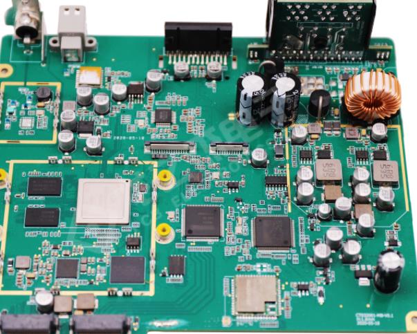

抖音二維碼

Q Q二維碼

微信二維碼
點擊
然后
聯系
然后
聯系
電話熱線
13410863085Q Q

微信

- 郵箱