鑫景福致力于滿足“快速服務,零缺陷,輔助研發”PCBA訂購單需求。


PCBA加工
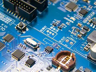
Factors Affecting PCBA cleaning and PCBA Generation
Influencing factors PCBs processing and cleaning
In a PCB chip processing plant, in order to make the cleaning of printed circuit components go smoothly and achieve good results, it is necessary to be familiar with not only the cleaning mechanism, cleaning agents and cleaning methods, but also the main factors that affect the cleaning effect, such as devICe type and layout, PCB design, flux type, welding process parameters, post welding dwell time, solvent spraying parameters, etc.
1 PCB design
During PCB design, it is necessary to avoid setting electroplated through-hole under components. In the case of wave soldering, the flux will flow to the upper surface of the shape memory alloy or below the patch on the upper surface of the shape memory alloy through the electroplated through-hole below the assembly, which will make it difficult to clean. The thickness and width of PCB should match each other and the thickness should be close. When wave soldering is selected, the thinner substrate must be reinforced with ribs or plates to increase the deformation resistance. This reinforcement structure will block the flux and is difficult to remove during cleaning. The welding mask shall be able to maintain good adhesion, and there shall be no microcracks or wrinkles after multiple welding.
2. Component type and layout
3. Flux type
The type of flux is the main factor affecting the cleaning of SMA after welding. As the percentage of solids in flux and the activity of flux increase, it becomes more difficult to clean flux residues. For specific shape memory alloy, which type of flux should be selected for welding must be considered in combination with the required cleanliness level of components and the cleaning process that can meet this level.
4. Reflow soldering process and post soldering dwell time
The influence of reflow soldering process on cleaning is mainly reflected in the temperature and residence time of preheating and reflow heating, which is the rationality of reflow heating curve. If the reflow heating curve is unreasonable, overheating of SMA will lead to flux deterioration, and it is difficult to clean the deteriorated flux. The residence time after welding refers to the residence time before the parts enter the cleaning process after welding, that is, the process residence time. During this period, the flux residue will gradually harden and cannot be removed. The residence time after welding shall be as short as possible. For specific shape memory alloys, the maximum allowable residence time must be determined according to manufacturing technology and flux type.
5. Spray pressure and speed
In order to better improve the cleaning efficiency and quality, spray washing is mostly used when static solvent or steam cleaning is selected. The use of high-density solvent and high-speed spraying can make the pollutant particles subject to greater force and easy to clean. However, when selecting the solvent, the density of the solvent is no longer a parameter that can be circLED, and the only adjustable parameter is the spray speed of the solvent.
Polychlorinated biphenyl generation treatment requirements
1、 Bill of Materials
The insertion or installation of components shall be carried out in strict accordance with the material list, PCB screen and outsourcing processing requirements. When the data do not conform to the bill of materials, PCB screen or process requirements, or the requirements are unclear and cannot be operated, we should be contacted immediately to confirm the accuracy of the data and process requirements.
2. Anti static requirements
1. All components are considered static sensitive devices.
2. All personnel contacting parts and products shall wear anti-static clothing, anti-static bracelets and anti-static shoes.
3. Static sensitive devices are selected for anti-static packaging of raw materials when entering the factory and warehousing.
4. During operation, use an anti-static working surface to store components and sEMI-finished products in anti-static containers.
5. The welding equipment shall be reliably grounded, and the electric soldering iron shall be anti-static. All products must pass the inspection before use.
6. Semi finished PCB boards are stored and transported in an anti-static box, and anti-static pearl cotton is used for isolation data.
7. The whole machine has no shell and uses anti-static packaging bag.
Third, specify the insertion direction of component appearance MARKs
1. Polar components are inserted by polarity.
2. For components with wire mesh on the side (such as high-voltage ceramic capacitors), when vertically inserted, the wire mesh faces the right side; When inserting horizontally, the silk screen shall face downward. When the components printed on the top (excluding chip resistors) are inserted horizontally, the font direction is the same as that of PCB screen printing; When inserting vertically, the upper side of the font faces right.
3. When the resistance is inserted horizontally, the error color ring goes to the right; When the resistance is inserted vertically, the error color ring is downward; When the resistor is inserted vertically, the error color ring faces the circuit board.
4、 Welding requirements
1. The pin height of 挿 part on the welding surface is 1.5 2.0mm. SMD components shall be flat pasted on the board surface, and the welding points shall be smooth, burr free and slightly arc-shaped. The solder shall exceed 2/3 of the height of the solder end, but shall not exceed the height of the solder end. Low tin, spherical solder joints or covered solder joints are unqualified products;
2. Height of solder joints: the height of solder studs for single panel solder joints shall not be less than 1mm, and the height of solder studs for double panel solder joints shall not be less than 0.5mm, requiring tin penetration.
3. Solder spot shape: conical, covering the entire pad.
4. Solder joint surface: smooth and bright, free of black spots, flux and other impurities, peaks, pits, pores, copper exposure and other defects.
5. Solder joint strength: completely wet with pads and pins, without faulty soldering or soldering
6. Solder joint section: the cutting leg of the component should not be cut to the solder as far as possible, and the contact surface between the lead and the solder should not have cracks. No barbs or barbs on the cross section.
7. Welding of needle seat: the needle seat must be installed at the bottom of the plate with correct position and direction. After the needle seat is welded, the bottom of the needle seat shall not float.
When it exceeds 0.5mm, the tilt of the seat shall not exceed the screen frame. The needle holders in rows shall also be kept in order, without dislocation or unevenness.
5、 Transportation
To prevent PCBs from being damaged, the following packaging should be used during transportation:
1. Storage container: anti-static turnover box.
2. Isolation data: anti-static pearl cotton.
3. Placement spacing: the distance between PCB boards and between PCB boards and boxes is greater than 10mm.
4. Placement height: there is a space of more than 50mm on the top of the turnover box to ensure that the turnover box will not be pressed on the power supply, especially the power supply of the electric wire.
6、 Plate washing requirements
The surface of the circuit board shall be clean, with no beads, component pins and stains. In particular, no dirt shall be left at the welding spot on the surface of the welding piece. When cleaning the distribution board, the following equipment shall be protected: wires, connection terminals, relays, switches, polyester capacitors and other easily corroded equipment. It is strictly prohibited to clean the relays with ultrasonic wave.
After installation, all components shall not exceed the edge of PCB board.
8. When polychlorinated biphenyls are above the furnace, because the pins of plug-in components are washed by the tin flow, some plug-in components will tilt after welding in the furnace, resulting in the part body exceeding the wire mesh frame Therefore, the maintenance and welding personnel behind the tin furnace need to perform correctly Repair
Influencing factors PCBs processing and cleaning
In a PCB chip processing plant, in order to make the cleaning of printed circuit components go smoothly and achieve good results, it is necessary to be familiar with not only the cleaning mechanism, cleaning agents and cleaning methods, but also the main factors that affect the cleaning effect, such as devICe type and layout, PCB design, flux type, welding process parameters, post welding dwell time, solvent spraying parameters, etc.
1 PCB design
During PCB design, it is necessary to avoid setting electroplated through-hole under components. In the case of wave soldering, the flux will flow to the upper surface of the shape memory alloy or below the patch on the upper surface of the shape memory alloy through the electroplated through-hole below the assembly, which will make it difficult to clean. The thickness and width of PCB should match each other and the thickness should be close. When wave soldering is selected, the thinner substrate must be reinforced with ribs or plates to increase the deformation resistance. This reinforcement structure will block the flux and is difficult to remove during cleaning. The welding mask shall be able to maintain good adhesion, and there shall be no microcracks or wrinkles after multiple welding.
2. Component type and layout

3. Flux type
The type of flux is the main factor affecting the cleaning of SMA after welding. As the percentage of solids in flux and the activity of flux increase, it becomes more difficult to clean flux residues. For specific shape memory alloy, which type of flux should be selected for welding must be considered in combination with the required cleanliness level of components and the cleaning process that can meet this level.
4. Reflow soldering process and post soldering dwell time
The influence of reflow soldering process on cleaning is mainly reflected in the temperature and residence time of preheating and reflow heating, which is the rationality of reflow heating curve. If the reflow heating curve is unreasonable, overheating of SMA will lead to flux deterioration, and it is difficult to clean the deteriorated flux. The residence time after welding refers to the residence time before the parts enter the cleaning process after welding, that is, the process residence time. During this period, the flux residue will gradually harden and cannot be removed. The residence time after welding shall be as short as possible. For specific shape memory alloys, the maximum allowable residence time must be determined according to manufacturing technology and flux type.
5. Spray pressure and speed
In order to better improve the cleaning efficiency and quality, spray washing is mostly used when static solvent or steam cleaning is selected. The use of high-density solvent and high-speed spraying can make the pollutant particles subject to greater force and easy to clean. However, when selecting the solvent, the density of the solvent is no longer a parameter that can be circLED, and the only adjustable parameter is the spray speed of the solvent.
Polychlorinated biphenyl generation treatment requirements
1、 Bill of Materials
The insertion or installation of components shall be carried out in strict accordance with the material list, PCB screen and outsourcing processing requirements. When the data do not conform to the bill of materials, PCB screen or process requirements, or the requirements are unclear and cannot be operated, we should be contacted immediately to confirm the accuracy of the data and process requirements.
2. Anti static requirements
1. All components are considered static sensitive devices.
2. All personnel contacting parts and products shall wear anti-static clothing, anti-static bracelets and anti-static shoes.
3. Static sensitive devices are selected for anti-static packaging of raw materials when entering the factory and warehousing.
4. During operation, use an anti-static working surface to store components and sEMI-finished products in anti-static containers.
5. The welding equipment shall be reliably grounded, and the electric soldering iron shall be anti-static. All products must pass the inspection before use.
6. Semi finished PCB boards are stored and transported in an anti-static box, and anti-static pearl cotton is used for isolation data.
7. The whole machine has no shell and uses anti-static packaging bag.
Third, specify the insertion direction of component appearance MARKs
1. Polar components are inserted by polarity.
2. For components with wire mesh on the side (such as high-voltage ceramic capacitors), when vertically inserted, the wire mesh faces the right side; When inserting horizontally, the silk screen shall face downward. When the components printed on the top (excluding chip resistors) are inserted horizontally, the font direction is the same as that of PCB screen printing; When inserting vertically, the upper side of the font faces right.
3. When the resistance is inserted horizontally, the error color ring goes to the right; When the resistance is inserted vertically, the error color ring is downward; When the resistor is inserted vertically, the error color ring faces the circuit board.
4、 Welding requirements
1. The pin height of 挿 part on the welding surface is 1.5 2.0mm. SMD components shall be flat pasted on the board surface, and the welding points shall be smooth, burr free and slightly arc-shaped. The solder shall exceed 2/3 of the height of the solder end, but shall not exceed the height of the solder end. Low tin, spherical solder joints or covered solder joints are unqualified products;
2. Height of solder joints: the height of solder studs for single panel solder joints shall not be less than 1mm, and the height of solder studs for double panel solder joints shall not be less than 0.5mm, requiring tin penetration.
3. Solder spot shape: conical, covering the entire pad.
4. Solder joint surface: smooth and bright, free of black spots, flux and other impurities, peaks, pits, pores, copper exposure and other defects.
5. Solder joint strength: completely wet with pads and pins, without faulty soldering or soldering
6. Solder joint section: the cutting leg of the component should not be cut to the solder as far as possible, and the contact surface between the lead and the solder should not have cracks. No barbs or barbs on the cross section.
7. Welding of needle seat: the needle seat must be installed at the bottom of the plate with correct position and direction. After the needle seat is welded, the bottom of the needle seat shall not float.
When it exceeds 0.5mm, the tilt of the seat shall not exceed the screen frame. The needle holders in rows shall also be kept in order, without dislocation or unevenness.
5、 Transportation
To prevent PCBs from being damaged, the following packaging should be used during transportation:
1. Storage container: anti-static turnover box.
2. Isolation data: anti-static pearl cotton.
3. Placement spacing: the distance between PCB boards and between PCB boards and boxes is greater than 10mm.
4. Placement height: there is a space of more than 50mm on the top of the turnover box to ensure that the turnover box will not be pressed on the power supply, especially the power supply of the electric wire.
6、 Plate washing requirements
The surface of the circuit board shall be clean, with no beads, component pins and stains. In particular, no dirt shall be left at the welding spot on the surface of the welding piece. When cleaning the distribution board, the following equipment shall be protected: wires, connection terminals, relays, switches, polyester capacitors and other easily corroded equipment. It is strictly prohibited to clean the relays with ultrasonic wave.
After installation, all components shall not exceed the edge of PCB board.
8. When polychlorinated biphenyls are above the furnace, because the pins of plug-in components are washed by the tin flow, some plug-in components will tilt after welding in the furnace, resulting in the part body exceeding the wire mesh frame Therefore, the maintenance and welding personnel behind the tin furnace need to perform correctly Repair

抖音二維碼

Q Q二維碼

微信二維碼
點擊
然后
聯系
然后
聯系
電話熱線
13410863085Q Q

微信

- 郵箱