鑫景福致力于滿足“快速服務,零缺陷,輔助研發”PCBA訂購單需求。


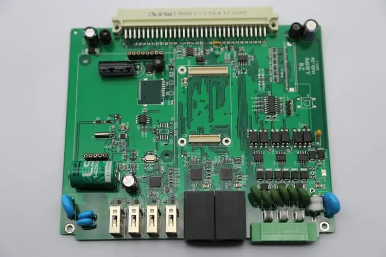
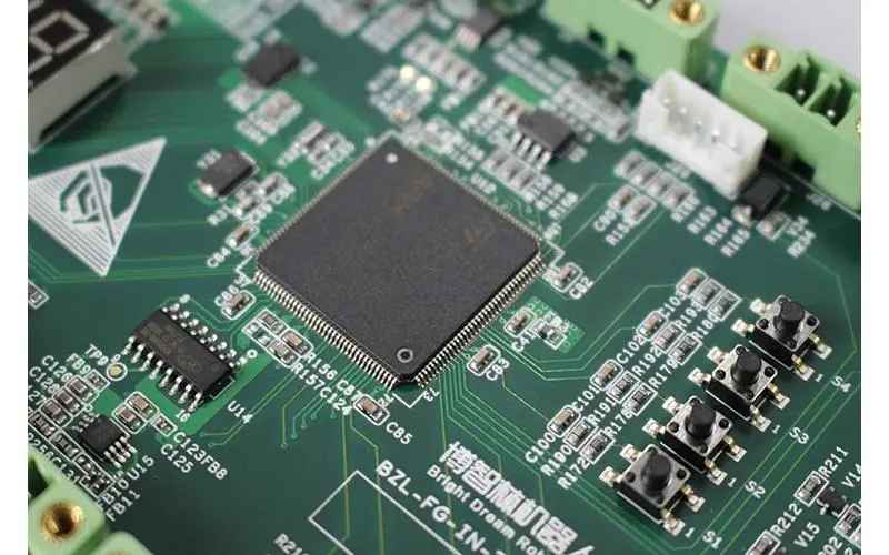
PCBA加工
AutomatIC Optical Inspection (AOI) system is usually used to test the inner layer before layering; After layering, the X-ray system monitors the accuracy of alignment and SMAll defects; The scanning laser system provides a method for detecting PCB pad layers before reflow. These systems, together with the production line straight
Automatic Optical Inspection (AOI) system is usually used to test the inner layer before layering; After layering, the X-ray system monitors the accuracy of alignment and small defects; The scanning laser system provides a method for detecting the pad layer before reflow. These systems, together with the visual inspection technology of the production line and the component integrity inspection for automatically placing PCB components, help to ensure the reliability of the final assembly and welding plate.
However, even if these efforts minimize the defects, the final inspection of the assembled PCB is still required, which is perhaps the most important, because it is the final unit of the product and the entire process evaluation.
The final inspection of PCB assembly may be completed by dynamic methods or by automatic systems, and often both methods are used. "Manual" means that an operator uses an optical instrument to visually inspect the board and make a correct judgment about the defect. The automatic system uses computer aided graphic analysis to determine defects. Many people also believe that the automatic system includes all detection methods except manual light detection.
X-ray technology provides a method to evaluate the solder thickness, distribution, internal cavities, cracks, desoldering and the presence of solder balls (MARKstein, 1993). Ultrasonics will detect cavities, cracks, and unbonded interfaces. Automated optical inspection evaluates external features such as bridging, tin flux, and shape. Laser detection can provide three-dimensional images of external features. Infrared detection detects internal solder joint failure by comparing the thermal signal of the solder joint with a known good solder joint.
It is worth noting that all defects that cannot be found by these automatic detection technologies in the limited detection of assembled printed circuit boards have been found. Therefore, manual visual inspection methods must be combined with automatic inspection methods, especially for those few applications. The combination of X-ray inspection and manual optical inspection is the best method to detect PCB assembly defects.
printed circuit boards assembLED and welded are prone to the following defects:
1) Missing components; 2) Component failure; 3) There is installation error and misalignment of components; 4) Component failure; 5) Poor tin adhesion; 6) Bridging; 7) Insufficient soldering tin; 8) Excessive solder to form solder balls; 9) Forming welding pinholes (bubbles); 10) Contaminants; 11) Improper pads; 12) Wrong polarity; 13) Pin floating; 14) The pin extends too long; 15) Cold welding contact occurs; 16) Excessive soldering tin; 17) Solder cavity; 18) There are blowholes; 19) The structure of the inner circle fillet of the printed wire is poor.
Introduction to Automatic Detection Technology of PCB
In complex PCB testing, two common methods are needle bed testing and double probe or flying probe testing.
1. Needle bed test method
This method is connected to each detection point on the circuit board by a probe with a spring. The spring makes each probe have a pressure of 100 - 200g to ensure good contact of each detection point. Such probes are arranged together and called "needle bed". Under the control of the detection software, the detection points and detection signals can be programmed. Figure 14-3 is a typical structure of the needle bed tester. The detector can obtain the information of all test points. In fact, only the probes at the test points that need to be tested are installed. Although the needle bed test method may be used to test both sides of the circuit board at the same time, when designing the circuit board, all the test points should be on the welding surface of the circuit board. Needle bed tester is expensive and difficult to maintain. The probes with different arrangements are selected according to their specific applications.
A basic universal grid processor is composed of a PCB drilling board, and the center spacing of the pins on the board is 100, 75, or 50 mil. The pin acts as a probe and uses the electrical connector or node on the circuit board for direct mechanical connection.
If the pad on the circuit board matches with the test grid, the polyacrylate film perforated according to the specification will be placed between the grid and the circuit board to facilitate the design of specific detection. Continuity detection is achieved by accessing the end point of the grid (defined as the x-y coordinate of the PCB pad). Since each network on the circuit board is tested for continuity. In this way, an independent detection is completed. However, the proximity of the probe limits the effectiveness of the needle bed test method.
2. Double probe or flying probe test method
The flying probe tester does not depend on the pin pattern installed on the fixture or bracket. Based on this system, two or more probes are mounted on a free moving micro magnetic head on the x-y plane, and the test points are directly controlled by the CADIGerber data. The double probes can move within a distance of 4mil from each other. The probes can move independently without really limiting how close they are to each other. The tester with two movable arms is based on capacitance measurement. Press the circuit board tightly and place it on the insulating layer of a metal plate as another metal plate of the capacitor. If there is a short circuit between lines, the capacitance will be greater than at a certain point. If there is an open circuit, the capacitance will decrease.
Test speed is an important standard for selecting a tester. The needle bed tester can accurately test thousands of test points at a time, while the flying needle tester can only test two or four test points at a time. In addition, the needle bed tester may only spend 20 - 305 for single side testing, which depends on the complexity of the board, while the flying needle tester requires IH or more time to complete the same evaluation. Shipley (1991) explained that even though manufacturers of high-yield printed circuit boards think that the mobile flying probe testing technology is slow, this method is still a good choice for manufacturers of low yield complex circuit boards.
For bare board testing, there are special testing instruments (Lea, 1990). A more cost optimized method is to use a general instrument. Although this kind of PCB instrument is more expensive than the special instrument at first, its initial high cost will be offset by the reduction of individual configuration costs. For the general grid, the standard grid for boards with pin components and surface mount devices is 2.5mm. At this time, the test pad should be greater than or equal to 1.3mm. For the Imm grid, the test pad PCB should be designed to be greater than 0.7mm. If the grid is small, the test pin is small, brittle and easy to damage. Therefore, grids larger than 2.5mm are preferred. Crum (1994b) clarified that the combination of a universal tester (standard grid tester) and a flying probe tester can make the detection of high-density circuit boards accurate and economical. Another method he suggests is to use a conductive rubber tester, which can be used to detect points that deviate from the grid. However, the height of pads leveled by hot air is different, which will hinder the connection of test points.
Three levels of automatic detection technology
1. Bare plate detection;
2. Online detection;
3. Function test.
The universal tester can be used to test a class of style and type of circuit boards, and can also be used for testing special applications.

抖音二維碼

Q Q二維碼

微信二維碼
點擊
然后
聯系
然后
聯系
電話熱線
13410863085Q Q

微信

- 郵箱