鑫景福致力于滿足“快速服務,零缺陷,輔助研發”PCBA訂購單需求。


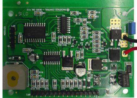
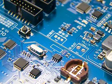
PCBA加工
A New Method to Reduce Cavity in SMT Processing
It is well known that welding large flat and low foot height components can create voids, such as QFN components The use of these types of components is being added In order to meet IPC standards, the formation of voids has attracted the attention of many designers. Operators and quality control personnel of SMT chip production line feel headache This paper will focus on a new method to reduce voids
When we carefully observe the solder joints and cavities, one of the main parameters does not seem to attract people's attention. This is a solder alloy. As a preliminary test, the three lead-free solder alloys commonly used in the MARKet all have the characteristICs of pore behavior.
Further research strategies include the use of tin, bismuth, silver, zinc, copper and other elements to adjust these alloys and observe their effects on the void behavior. Since this method can rapidly produce many alloys, this TGA analysis is used as an initial selection tool. Thermogravimetric analysis can be used to monitor the evaporation of the chEMIcal components of the flux and the reflow temperature distribution during the bonding with an alloy. Experience shows that a smoother evaporation curve usually means a lower level of pore formation. From this study, eight prototype solder alloys were selected and their void behavior was characterized.

To this end, 60 QFN coated with each alloy were welded on three different coated substrates: NiAu (ENIG), OSP and I-Sn. The chemical composition, template thickness and layout and substrate layout of the solder paste used in all alloys are the same. Use the welding temperature curve according to the melting point of the alloy. X-ray is used to determine the void content level. One of the alloys obtained the best results in terms of cavitation behavior and was selected for further mechanical reliability testing.
1. Introduction
For many years, the mechanism of void formation in solder joints has been the subject of research. Many void types and formation mechanisms have been identified. The most striking is the huge gap. It seems that the main factor for forming large voids is the chemical composition of the solder paste.
Micropores, shrinkage cavities and Kirkendall cavities are also well known types of cavities, but they are beyond the scope of this paper. Over the years, many technologies have been established to reduce the formation of voids.
Adjusting the chemical composition of solder paste, reflow soldering temperature curve, components, PCB and template design or coating are some optimization tools currently widely used SMT chip proofing manufacturers Even equipment manufacturers are offering solutions to reduce porosity through sweep or vacuum technology However, another very important parameter defines the pore formation of the welding alloy
Welding alloy: an unusual and suSPIcious factor. The main cause of cavity formation has been considered to be the flux in the solder paste. It seems to be the right way to design a solder paste flux that can effectively reduce voids, because about 50% of the flux will evaporate during reflow, resulting in voids. As the focus of the research is solder paste flux, so far, the research on the difference of void formation of different solder alloys has not attracted enough attention.
Use standard weldable alloys to measure the void level to determine the baseline void formation percentage, such as SnAg3Cu0.5 (SAC305), SnAg0.3Cu0.7 (LowSAC0307), and Sn42Bi57Ag1. All tests described in this document use the same paste chemistry.
In order to understand the level difference between PCB coatings, three coatings commonly used in industry were tested: OSPCu, ENIG (NiAu) and I-Sn. In order to have enough clearance, a sample of 120mm was used without reducing the gasket. For each solder paste, 60 tin coated QFN components are reflowed using the standard heating reflow curve applicable to each specific solder alloy.
X-ray inspection shall be carried out for each component, and the pore level in the ground plane shall be measured to determine the percentage of pores. The percentage of voids is calculated by comparing the void area with the ground level area. The size of a single cavity is not considered. The test results show that the results of SAC305 and LowSAC0307 are quite poor. Sn42Bi57Ag1 achieved better results.
2. Alloy optimization
Based on these test results, the research scheme of the best welding alloy is formulated from the perspective of porosity efficiency. Thermogravimetric analysis and X-ray analysis were used for the study protocol. In addition, other parameters such as reflux temperature distribution, yield strength, viscosity range, elongation and other process parameters are also considered.
The R&D strategy includes starting from the standard lead-free solder alloy and adjusting it with tin, bismuth, silver, zinc, copper, etc. This quickly produced many candidate alloys, and TGA analysis was used as an initial selection tool. Thermogravimetric analysis can be used to monitor the evaporation of the chemical components of the flux and the reflow temperature distribution during the bonding with an alloy. A smoother evaporation curve usually implies a lower level of pore formation. Eight prototype solder alloys were selected for further study.
3. Eight prototype solder alloys
The same test settings as the initial benchmark were performed on 8 prototype solder alloys This means that each solder paste is used to weld QFN on different PCB finishes, and X-ray is used to analyze the real pore characteristics The preliminary test results show that, compared with the standard alloy SAC305, the porosity level of LowSAC0307 and Sn42Bi57Ag1 is significantly reduced The test alloy G has the lowest void ratio and narrowest propagation results
The alloy was selected for further mechanical reliability testing.
Compared with SAC305, it not only has a lower void fraction efficiency, but also has a good impact resistance, vibration resistance and hot loop performance. In addition, in addition to reflow welding, the alloy has also been proven to be suitable for wave soldering and selective welding. Alloy G will be named LMPA-Q and will be commercialized.
The above is the explanation given by the editor of pcb circuit board company.
If you want to know more about PCBA, you can go to our company's home page to learn about it.
In addition, our company also sells various circuit boards,
High Frequency Circuit Board and SMT chip are waiting for your presence again.


抖音二維碼

Q Q二維碼

微信二維碼
點擊
然后
聯系
然后
聯系
電話熱線
13410863085Q Q

微信

- 郵箱