鑫景福致力于滿足“快速服務(wù),零缺陷,輔助研發(fā)”PCBA訂購(gòu)單需求。


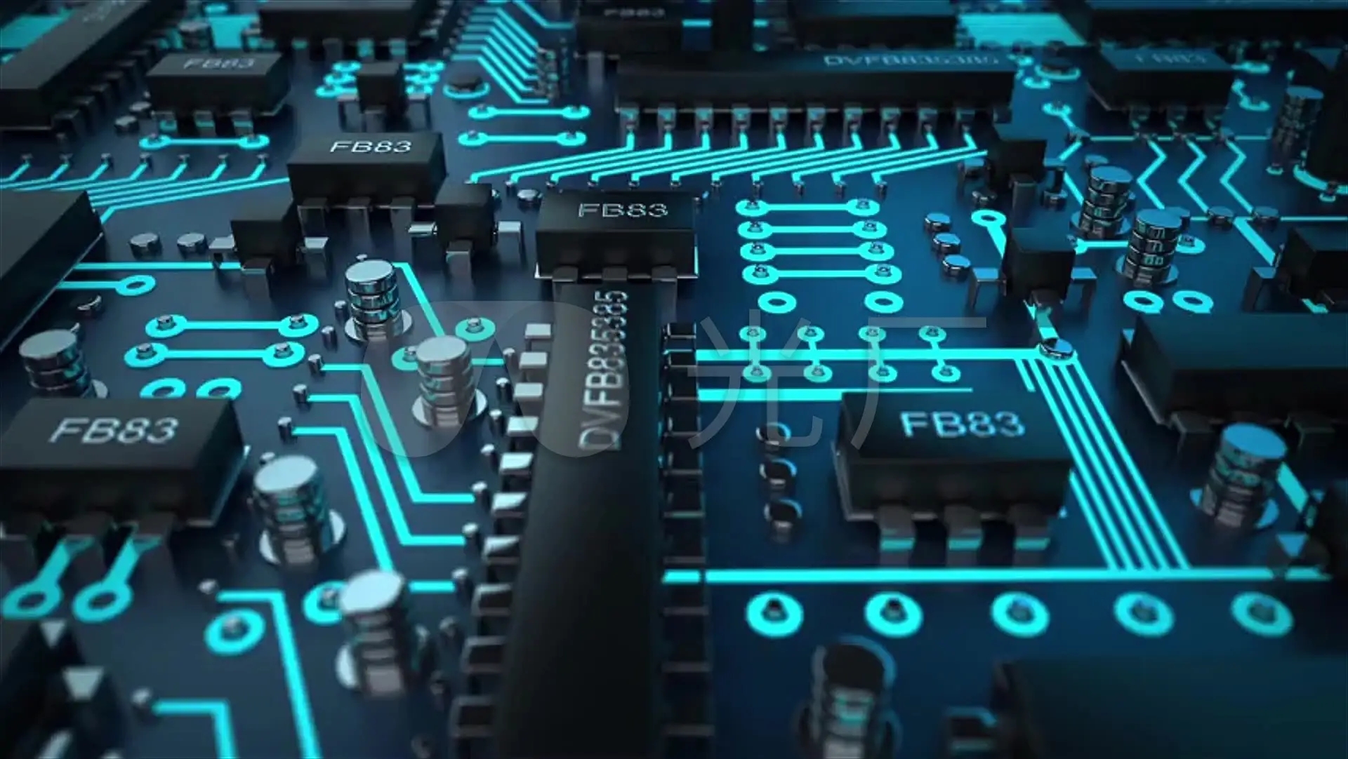
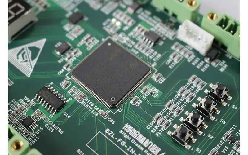
PCBA加工
Description method is to manufacture the circuit board requires the least tools, manufacturing process is the SIMplest of a method, but the accuracy is not very high, suitable for beginners.

1. Draw PCB diagram on Protel software.
2. Print with a printer.
3. Prepare copper-clad plates of the same size.
4. Take a piece of carbon paper (similar to the blue paper used for issuing invoICes) and carbon write the PCB diagram printed on the ordinary white paper to the copper plate through the ballpoint pen.
5. Description, take a very fine oil MARKer to describe the lines that have just been copied to the copper plate. For those that are not obvious enough at one time, you can repeat the description to ensure that the lines of the description part are not broken. It is also important to note that care must be taken when drawing pcb diagrams to prevent careless gluing of otherwise disjoint lines.
6, the configuration of corrosion solution on the circuit board corrosion, you can use electrolysis, hydrogen peroxide + concentrated hydrochloric acid + water, ferric chloride solution and other methods to corrosion copper clad plate.
7, with a drilling machine to drill the circuit board, we recommend the use of micro bench drill drilling precision.
Two, the photographic plate method
It is easy to manufacture, especially when the ground line is large area. Accuracy is high, but exposure for thin lines requires experience.
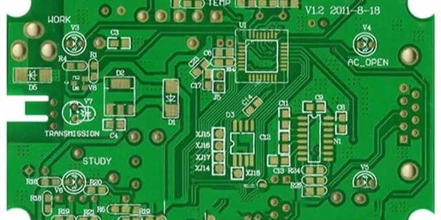
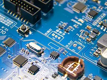
PCB circuit board production process
●PCB(printed circuit board) is made of fiberglass, a material we can see in everyday life, such as
The core of fireproof cloth and fireproof felt is glass fiber. Glass fiber is easy to combine with resin. We immerse the glass fiber cloth with tight structure and high strength in resin, and harden it to get the thermal insulation and not easy to bend the PCB substrate. If the PCB board is broken, the edge is white and layered, which is enough to prove that the material is resin glass fiber.
● We cannot transmit electrical signals on the insulation board alone, so we need to cover the surface with copper. So we call the PCB board
Is copper-clad substrate. In the factory, the common copper-clad substrate code is FR-4, which is generally not different in eachr board manufacture, so we can think that everyone is on the same starting line, of course, if it is high frequency board, it is best to use the higher cost of copper-clad polytetrafluoroethylene glass cloth laminate.
Copper coating process is very simple, generally can be made by calendering and electrolysis, the so-calLED calendering is the high purity
(> 99.98%) of copper is pasted on PCB substrate by rolling method -- because epoxy resin has excellent adhesion with copper foil, copper foil has high adhesion strength and working temperature, and can be immersed in tin at 260℃ without foaming.
● the process is much like rolling dumpling skins, which can be as thin as 1mil or less
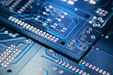
When in 0.0254 mm). If the dumpling skin is so thin, the pot will surely leak the filling! The so-called electrolytic copper has been learned in junior high school chEMIstry, CuSO4 electrolyte can constantly produce layers of "copper foil", so it is easy to control the thickness, the longer the copper foil is thicker! Usually the factory has very strict requirements on the thickness of copper foil, generally between 0.3mil and 3mil, there is a special copper foil thickness tester to test its quality. PCBs, like old radios and hobbyists, are covered with thick copper, far less quality than those found in computer card factories.

● Control of copper foil thinness is mainly based on two reasons: one is uniform copper foil can have a very uniform resistance temperature
This is different from capacitance, which requires a high permittivity in order to accommodate a higher capacity in a finite volume. The reason why resistance is SMAller than capacitance is that it has a high permittivity.
Secondly, the temperature rise of thin copper foil through large current is small, which is of great benefit to heat dissipation and component life. The width of copper wire in digital integrated circuit is best less than 0.3cm. A well-made finished PCB is very uniform and has a soft sheen (because of the flux brush), which can be seen by the naked eye, but not many people can tell the difference by looking at a copper-clad substrate, unless you are an experienced inspector in the factory.
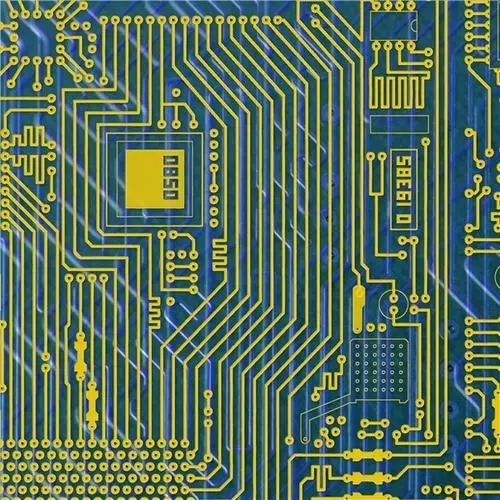
● For a whole body wrapped copper foil PCB substrate, how can we place components on it, to achieve components - yuan
What about the signal conduction between pieces instead of the whole board? The winding copper wire on the board is used to realize the transmission of electrical signals. Therefore, we just need to corrode the copper foil and leave the copper wire part.
So that's the circuit board manufacturing process, and we can learn from the circuit board manufacturing process in many places.

抖音二維碼

Q Q二維碼

微信二維碼
點(diǎn)擊
然后
聯(lián)系
然后
聯(lián)系
電話熱線
13410863085Q Q

微信

- 郵箱