鑫景福致力于滿足“快速服務,零缺陷,輔助研發”PCBA訂購單需求。


行業新聞
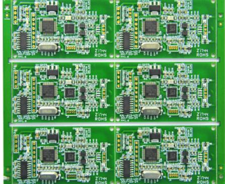
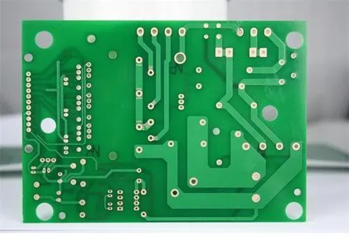
What is the PCBA inspection standard of SMT factory?
Shenzhen PCBA manufacturer will take you familiar with some PCBA production processes of SMT technology workshop What are the inspection requirements for PCBA proofing in SMT technology chip processing workshop during production?
1. First, the pre production data of SMT process workshop
Smt related technICal operators check the specification, model and size of the base plate according to the PCBA proofing product patch processing or feeding specification drawings. The longitude and latitude direction, length and width dimensions and perpendicularity of the base plate are within the range specified in the drawing.
2. Smt technology equipment starts printing screen plate: first, check whether the MESh, screen tension and film thickness meet the requirements; Then check the integrity of the pattern without pinholes, gaps or residual films; Use Photo Gallery to check that graphics are aligned on size, line width, line spacing, connector tile size, or character tags.

3. Surface cleaning: The surface of PCBA board after chEMIcal cleaning shall not be oxidized or polluted, and shall be dry after cleaning.
Polychlorinated biphenyls
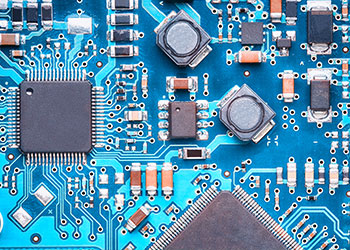
4. Printing requirements PCBA board: check the graphic integrity of lines, uninterrupted, pinhole, gap or short circuit; Check the photo background, graphics size alignment, line width and line spacing, and the error is within the allowable range
5. Etching of PCBA circuit board: check the graphic integrity of the circuit, without fracture, pinhole, gap or short circuit; Check with photo negative, there is no etching (the line is too thin) or insufficient etching (the line is too thick).
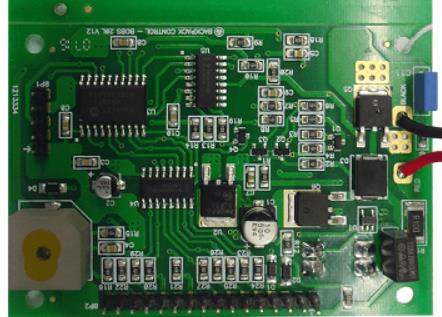
6 PCBA circuit board resistance: check the integrity of the resistance pattern, no leakage, pinholes, notches or ink penetration, excessive ink spots on the upper brake disc; It is consistent with the positioning size of line graphics, and the error is within the allowable range Then continue to check the curing degree of the solder The solder layer on the copper conductor surface shall be tested with a pencil The hardness of the pencil should be greater than 3H Finally, check the welding adhesion PCBA circuit board The welding layer PCBA plate on the copper conductor surface shall be bonded and pulLED up with adhesive tape There should be no peeling solder on the tape
7. Character MARK PCBA circuit board on the front and back: the relevant person in charge of SMT product inspection department strictly checks the graphic integrity of character mark on the machine. PCBA boards meet the implementation standards, and there is no fingerprint, pinhole, gap or ink penetration, electroplating or additional ink spots; It is consistent with the positioning size of the line graph, and the error is within the allowable range, and the character mark can be correctly identified


抖音二維碼

Q Q二維碼

微信二維碼
點擊
然后
聯系
然后
聯系
電話熱線
13410863085Q Q

微信

- 郵箱