鑫景福致力于滿足“快速服務,零缺陷,輔助研發”PCBA訂購單需求。


行業新聞
design skills and key points for realizing advanced automatIC PCB routing
Although EDA tools are very powerful, PCB design is not easy as PCB size requirements become SMAller and smaller and device density becoMES higher and higher. How to achieve high PCB routing rate and shorten the design time? This paper introduces the design skills and key points of PCB planning, layout and routing.
Now the time for PCB design is getting shorter and shorter, the smaller and smaller PCB space, the higher and higher device density, the extremely strict layout rules and large size components make the work of designers more difficult. In order to solve the design difficulties and speed up the launch of products, many manufacturers now tend to use special EDA tools to achieve PCB design. However, the special EDA tool can not produce ideal results, nor can it achieve 100% of the deployment rate, and it is very messy, and it usually takes a lot of time to complete the rest of the work.
There are many popular EDA tool software on the MARKet, but they are almost the same except for the different terminology and function key positions. How can we use these tools to better realize PCB design? The careful analysis of the design and the careful setting of the tool software before the start of wiring will make the design more consistent with the requirements. The following is the general design process and steps.
1. Determine the number of layers of PCB
The size of the circuit board and the number of wiring layers need to be determined at the initial stage of design. If the design requires the use of high-density ball grid array (BGA) components, the minimum number of wiring layers required for the wiring of these devices must be considered. The number of wiring layers and the stacking up method will directly affect the wiring and impedance of the printed wire. The size of the board is helpful to determine the stacking mode and the width of the printed line to achieve the desired design effect.
For many years, people have always believed that the lower the number of circuit boards, the lower the cost. However, there are many other factors that affect the manufacturing cost of circuit boards. In recent years, the cost difference between multilayer boards has been greatly reduced. At the beginning of the design, it is better to use more circuit layers and make the copper coating evenly distributed, so as to avoid that a small number of signals do not meet the defined rules and space requirements when the design is near the end, so that new layers are forced to be added. Careful planning before design will reduce a lot of trouble in cabling.
2. Design rules and restrictions
The auto routing tool itself does not know what to do. To complete the routing task, the routing tool needs to work under the correct rules and restrictions. Different signal lines have different wiring requirements. All signal lines with special requirements should be classified, and different design classifications are also different. Each signal class should have a priority. The higher the priority, the stricter the rules. The rules involve the width of printed wire, the maximum number of vias, parallelism, the interaction between signal wires, and layer restrictions. These rules have a great impact on the performance of wiring tools. Careful consideration of design requirements is an important step for successful cabling.
To optimize the assembly process, design for manufacturability (DFM) rules impose restrictions on component layout. If the assembly department allows the components to move, the circuit can be properly optimized to facilitate automatic wiring. The rules and constraints defined affect the layout design.
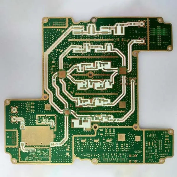
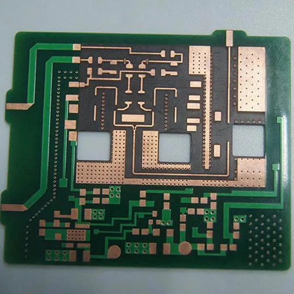
The routing channel and via area shall be considered in the layout, as shown in Figure 1. These paths and areas are obvious to designers, but the automatic routing tool will only consider one signal at a time. By setting the routing constraint conditions and setting the layers of signal wires that can be routed, the routing tool can complete the routing as envisioned by the designer.
4. Fan out design
In the fan out design stage, to enable the automatic wiring tool to connect the component pins, each pin of the surface mount device should have at least one via, so that when more connections are needed, the circuit board can conduct internal connection, online test (ICT) and circuit reprocessing.
In order to maximize the efficiency of the automatic routing tool, it is necessary to use the largest via size and printed wire as much as possible, and it is ideal to set the spacing at 50mil. Use the type of vias that maximize the number of routing diameters. When fan out design is carried out, the problem of circuit online test should be considered. Test fixtures can be expensive and are usually ordered when they are about to go into full production. It is too late to consider adding nodes to achieve 100% testability.
After careful consideration and prediction, the design of circuit online test can be carried out at the initial stage of design and realized at the later stage of production process. The type of via fan out can be determined according to the wiring path and circuit online test. The power supply and grounding will also affect the wiring and fan out design. In order to reduce the inductance generated by the connecting line of the filter capacitor, the vias should be as close to the pins of surface mount devices as possible. If necessary, manual wiring can be used. This may affect the originally envisaged wiring path, or even cause you to reconsider which vias to use. Therefore, the relationship between vias and pin inductance must be considered and the priority of vias specification must be set.
5. Manual wiring and key signal processing
Although this paper mainly discusses the problem of automatic routing, manual routing is an important process of PCB design now and in the future. Manual routing is helpful for automatic routing tools. By manually routing and fixing the selected network (net), a path that can be used for automatic routing can be formed.
No matter how many key signals are, these signals can be wired first, either manually or with automatic wiring tools. The key signals usually have to be carefully designed to achieve the desired performance. After wiring, it is much easier for relevant engineers to check these signal wiring. After passing the inspection, fix these lines, and then start to automatically route the rest of the signals.
6. Automatic wiring
For the wiring of key signals, it is necessary to consider controlling some electrical parameters during wiring, such as reducing the distributed inductance and EMC, etc. The wiring of other signals is SIMilar. All EDA manufacturers will provide a method to control these parameters. The quality of automatic routing can be guaranteed to a certain extent after knowing what input parameters the automatic routing tool has and the impact of the input parameters on routing.
General rules should be used to automatically route signals. By setting limiting conditions and prohibited wiring areas to limit the layers used for a given signal and the number of vias used, the wiring tool can automatically wire according to the design idea of the engineer. If there is no limit on the number of layers and vias used by the automatic routing tool, each layer will be used during automatic routing, and many vias will be generated.
After setting the constraints and applying the rules created, the automatic routing will achieve similar results as expected. Of course, some sorting work may be required, as well as ensuring the space for other signals and network routing. After part of the design is completed, fix it to prevent it from being affected by the later wiring process.
Use the same procedure to route the remaining signals. The number of wiring depends on the complexity of the circuit and the number of general rules you define. After each type of signal is completed, the constraints of other network routing will be reduced. However, many signal wiring needs manual intervention. Today's auto routing tools are very powerful, and can usually complete 100% routing. However, when the automatic wiring tool has not completed all signal wiring, it is necessary to manually wire the remaining signals.
The design points of automatic routing include: 1. Change the settings slightly, and try multiple routing paths; 2. Keep the basic rules unchanged, try different wiring layers, different printed lines and spacing widths, different line widths and different types of vias, such as blind holes and buried holes, and observe how these factors affect the design results; 3. Let the wiring tool handle the default networks as needed; 4. The less important the signal is, the more freedom the automatic routing tool has for its routing.
7. Arrangement of wiring
If the EDA tool software you use can list the signal wiring length and check these data, you may find that some signal wiring lengths with few constraints are very long. This problem is relatively easy to handle. By manual editing, the signal wiring length can be shortened and the number of vias can be reduced. In the sorting process, you need to judge which wiring is reasonable and which is unreasonable. Like manual routing design, automatic routing design can also be organized and edited during inspection.
8. Appearance of circuit board
In the past, the design often paid attention to the visual effect of the circuit board, but now it is different. The circuit board designed automatically is not more beautiful than that designed manually, but it can meet the specified requirements in terms of electronic characteristics, and the complete performance of the design is guaranteed.


抖音二維碼

Q Q二維碼

微信二維碼
點擊
然后
聯系
然后
聯系
電話熱線
13410863085Q Q

微信

- 郵箱