鑫景福致力于滿足“快速服務,零缺陷,輔助研發”PCBA訂購單需求。


行業新聞
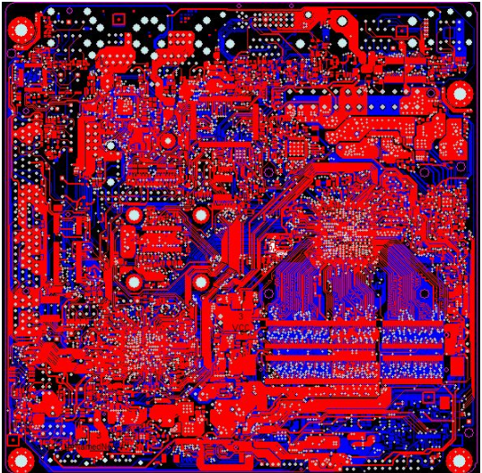
PCB design is a key and time-consuming task, and PCB engineers are required to check the whole network and component by component in case of any problem. It can be said that the degree of care required by circuit board design is no less than that of chip design. A typICal circuit board design process consists of the following steps:
The first three steps take the most time because schematic checking is a manual process. Imagine a SoC board with 1000 or more connections. Checking each connection manually is a tedious task. In fact, it is almost impossible to check each connection, which will eventually lead to problems on the circuit board, such as incorrect connections and suspended nodes.
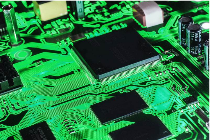
Circuit board design
PCB schematic diagram capture phase generally faces the following types of problems:
Underline error: such as APLLVDD and APLL_ VDD
Case problems: such as VDDE and vdde, spelling errors, signal short circuit, etc
To avoid these errors, there should be a way to check the complete PCB schematic diagram in a few seconds. This method can be realized by PCB schematic SIMulation, which is rarely seen in the current PCB design process. The final output results can be observed at the required nodes through PCB schematic simulation, so it can automatically check all connection problems. The following is an example of a project. Consider a typical block diagram of the circuit board:
In a complex PCB design, the number of wires may reach thousands, and a few changes may waste a lot of time to check. Schematic simulation can not only save design time, but also improve the quality of the circuit board, and improve the efficiency of the whole process.
A typical equipment to be tested has the following signals:
The PCB device to be tested will have various signals after some pre adjustments, and there are various modules, such as voltage regulator, operational amplifier, etc., for signal adjustment. Consider an example of power supply signal obtained through the voltage regulator:
To verify connectivity and perform an overall check, schematic simulations are used. Schematic simulation consists of schematic diagram creation, test platform creation and simulation. During the creation of the test platform, the excitation signals are given to the necessary input terminals, and then the output results are observed at the signal points of interest. The above process can be achieved by connecting the probe to the node to be observed. The node voltage and waveform can indicate whether there is an error in the schematic diagram. All signal connections are checked automatically.
With the help of simulation, we can directly observe the results to confirm whether the schematic diagram of the circuit board is correct. In addition, the investigation of circuit Board Design changes can be realized by carefully adjusting the excitation signal or component value. Therefore, schematic simulation can save a lot of time for circuit board designers and inspectors, and increase the correctness of circuit board design.


抖音二維碼

Q Q二維碼

微信二維碼
點擊
然后
聯系
然后
聯系
電話熱線
13410863085Q Q

微信

- 郵箱