鑫景福致力于滿足“快速服務,零缺陷,輔助研發”PCBA訂購單需求。


行業新聞
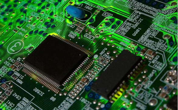
Advanced PCB manufacturing process brings high technICal threshold and yield test, which also drives equipment suppliers to update and evolve from laminators, screen printers, drilling machines to AOI equipment
Mobile device drives the application of FPC soft board and HDI high-density board
FPC soft board and relevant film pressing machine with flexible and easy three-dimensional structure characteristics.
The HDI&Anylayer HDI process uses a laser drilling machine.
Traditional hard boards (RPCBs) are hard, which limits the internal volume and modeling design of the terminal products. Flexible Print Circuit (FPC) CAMe into being. FPC soft boards can be divided into 2 layer FCCL without adhesive system and 3 layer FCCL with adhesive system according to the number of layers. The former is directly combined by Flexible copper foil substrate (FCCL) and flexible insulation layer, and has the advantages of high heat resistance, good flexure resistance, good dimensional stability, etc., but the cost is relatively high. Only higher level applications can use 2L FCCLFPC soft boards; 3L FCCL is made by pressing soft copper foil substrate and insulating layer through epoxy adhesive, which has low cost and is widely used.
The advantages of FPC soft board include light weight, flexibility, changing shape according to space to make stereo wiring, improving the wiring density of the system and reducing the product volume. At present, FPC soft boards are widely used in computers and peripherals, communication products, digital cameras, consumer electronics, automobiles, military and other fields, especially communication products and panels. Communication products account for about 30% of the total, followed by panels accounting for more than 20%, and PCs and peripherals accounting for 20%. The disadvantage is that it is easy to get stuck with dust due to electrostatic residue, and it is also easy to be damaged due to falling or collision during manufacturing, and it is not suitable for connecting heavy components.
FPC soft board can be subdivided into:
1. Single side: the most basic type of FPC soft board. A conductive layer is coated with a bonding layer, and then a dielectric layer is added.
2. Double side board: The double side board base material is used and a layer of covering film is added respectively. However, due to its thick thickness, the flexibility can be slightly reduced, which limits its application field.
3. Multilayer: It is mainly composed of single panel or double panel, and the conductive layer is connected through drilling; However, due to more layers and poor flexibility, its application field is limited;
4. Rigid Flex: It is composed of multi-layer hard boards plus single-sided FPC soft boards or double-sided FPC soft boards. It has the support of hard boards and the flexibility of FPC soft boards.
5. For example, single layer two side exposed plate (Double Acess), relief plate (Sculptural) and other special plates.
In addition, for the integration of mobile and wearable devices, FPC products have emerged, such as LCP-FPC, High density Multilayer FPC, optical waveguide FPC, waterproof FPC, transparent FPC, ultra-thin FPC, 3D forming FPC, Integral molding FPC, Stretchable FPC, ultra-fine line FPC, etc. For example, for SMArt watches or smart bracelets, thin lithium polymer batteries, MEMS sensors and FPCs are combined and embedded in the bracelet body or strap structure for three-dimensional folding and bending; Another example is the FPC designed for the vehicle electronic environment, which emphasizes the characteristics of high shock resistance and high heat resistance.
In order to meet the design trend of high efficiency, high transmission rate and active thinning, such as 5~10Gbps of high-speed connection interfaces such as USB 3.0/3.1/HDMI, 20Gbps of high-speed connection interfaces to telecom Netcom equipment to meet the needs of optical fiber transmission. FPCs supporting high-speed transmission applications are liquid crystal polymer (LCP) materials with low inductivity, supplemented by extended pressing range to 6~9 μ The ultra-thin copper foil material with thickness of m has reached the goal of supporting transmission, reducing skin effect in ultra-high frequency transmission process, and taking into account the need for thinness.
Taiwan FPC soft board technology originated from the technology of Japanese manufacturers in the early stage, and most of them played the role of a cooperative factory of Japanese manufacturers. Because of the high threshold for FPC soft board to enter, most of the investors quietly carried out under the table in the way of duck water skiing; When mobile phone OEM is achieved and becoMES the main business project of PCB, the application of FPC soft board is naturally accelerated.
When Intel, the leading processor manufacturer, launched CULV series Pentium III, Pentium M and other CPUs with Flip chip FC-BGA in 1998, it drove the PCB industry to move towards the light and thin notebook product line, and PCBFPC software board gradually expanded from consumer electronics to PC and communication fields. FPC soft board is already a necessary material for thin and light/extreme laptop, tablet computer and even smart phone. At the same time, the thinner the mobile device, the more pieces (dosage) of FPC soft board used. At present, Japan, South Korea and Taiwan are the main manufacturers of FPC soft boards in the world, and Taiwan's FPC soft board manufacturers include Jialianyi, Taijun, Yijia, Zhending, etc. The suppliers of FPC soft plate laminator equipment include Zhisheng Industry, Yazhi Technology, etc.
Laser drilling Tianyan constructs HDI giant tower with copper foil/FR4
When mobile devices and flat devices are moving towards high time pulse, multi-core and high efficiency, and product functions are becoming increasingly diversified and complex, both the number of electronIC components used or the number of contact pins of a single component are also increasing. At the same time, in response to the signal transmission requirements of high time pulse, they must meet the electrical characteristics and consider the signal impedance and avoid skin effect; It is also necessary to adapt to the transmission of wireless networks, and strive to improve RF signal optimization and avoid electromagnetic interference. More power layers and grounding layers must be added, so that the wiring space and design of circuit boards inevitably move from single layer, double layer, four layer and eight layer to multi layer PCB boards and even high density interconnect (HDI) PCBs.
HDI boards are manufactured by the Build Up method. Generally, HDI boards are basically made by adding layers once, while high-order HDI boards are made by adding layers twice (or more). At the same time, plating hole filling, hole stacking, laser direct drilling and other technologies are used. According to the definition of HDI board by the American circuit board Association, the specified aperture shall be less than or equal to 6mil, the ring diameter of ring or pad or land shall be less than or equal to 10 mil, the contact density shall be greater than 130 points/square inch, the wiring density shall be greater than 117 inches/square inch, and the line width/spacing shall be less than 3mil. Traditional mechanical drilling is easy to cause destructive problems such as cracking of pcb board. HDI was changed to Laservia laser drilling blind hole mode with good processing speed and quality, reaching (<150 μ m. 6mil) has become the mainstream in the industry. The problem mentioned above can be avoided by burning holes with optical lasers.
The iPhone 4 smartphone launched by Apple in June 2010 was the first to use any layer HDI process. The difference between any layer HDU and HDI is that, except for the upper and lower layers of HDI surface and bottom, the substrate of the middle layer can omit the use of the calendering copper foil substrate, and the blind holes can be directly drilLED through with high-power laser microdrills. Because the thickness of the copper foil substrate is omitted, the total thickness of the overall product becomes thinner. According to industry estimates, the overall volume of the terminal product can be reduced by about 40% when HDI is changed to any layer HDI.
As for laser drilling machine, the light sources used include 1.064 μ m red laser generated by solid neodymium chloride (Ng: YAG), 100~400 nm UV laser, and CO2 laser source of low-cost DLD process. In the early days, Canada Lumonics launched YAG-CO2, American ESI/German Siemens and others launched YAG-UV dual lasers, Israel Orbotech's UV laser drilling technology, and Nissan Hitachi, Panasonic, Takeuchi, Mitsubishi and others launched RF CO2 or CO2 laser systems.
Intelligent wearable PCB
Build independent technology of PCB industry and accelerate unified specification
In the past, due to the lack of mastery of laser processing technology by Taiwan PCB equipment factories, laser light sources almost all rely on imports. In order to improve the laser light source technology of the platform equipment business platform, after the Industrial Research Institute has also developed its own precision laser processing technology, the technology of the Southern Branch was transferred to Dongtai Precision Drilling Machine (Tongtai), and the TLC-2H22 CO2 laser drilling machine was launched μ CO2 laser light source with m wavelength, maximum average power of 350W, direct laser drilling (DLD), and less than 3 μ M, and less than 10 μ M scanning accuracy. Dongtai also cooperated with Dongjie Technology, a related enterprise, to establish a joint venture with Japanese Cyber Laser Inc. to establish Cyber Laser Taiwan, master the femtosecond laser light source technology, and vertically integrate various PCB manufacturing equipment from top to bottom.
As for the production of HDI and Anylayer HDI PCB products, there are Xinxing Electronics, Huatong Computer, Yaohua Electronics, and Jinxiang Electronics among the first tier large manufacturers with high process and yield. In addition to obtaining orders from Apple iPhone 6S in Anylayer HDI, other applications such as HDI and F-PCB in wearable devices and IoT devices are also increasing, and the proportion of shipments is increasing year by year. In response to the competition between the Internet of Things, the red supply chain on the opposite shore and the Korean and Japanese industries, TPCA actively invited PCB manufacturers and equipment manufacturers to hold a series of lectures on advanced PCB technology and equipment automation, and expected to use semiconductors such as wafers to replace industry, unify the communication specifications of upstream, midstream and downstream equipment, and build PCB equipment communication by combining production, learning and research resources.

抖音二維碼

Q Q二維碼

微信二維碼
點擊
然后
聯系
然后
聯系
電話熱線
13410863085Q Q

微信

- 郵箱