鑫景福致力于滿足“快速服務(wù),零缺陷,輔助研發(fā)”PCBA訂購(gòu)單需求。


行業(yè)新聞
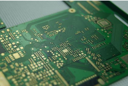
In the production and manufacturing stage of SMT chip processing plant, lead-free furnace processing technology has always been a very obvious PCB processing process supervision problem in production and processing. In the production process of SMT chip, lead-free solder joints with high quality can be produced. For the whole process of electronIC processing, they have an irreplaceable proactive effect. However, in the production and processing of lead-free reflow soldering furnace, there are also some production and processing problems that can not be ignored. It is this problem that has been harming electronic processing. Let's discuss this problem with you.
1、 Impact toughness of solder joint
Lead has high plasticity and soft color. Therefore, in SMT production and processing, because there is no lead added, the strength of lead-free solder joints is higher than that of Sn/Pb, and the compressive strength of lead-free solder joints is also higher than that of Sn/Pb. The deformation of lead-free solder joints is SMAller than that of Sn/Pb solder joints, but this does not mean that lead-free solder joints in PCBA are always good, and the long-term reliability is uncertain.
Most consumer goods, such as civil and communication industries. Because the application of natural environment does not have great geostress. The impact toughness of lead-free solder joints is even higher than that of lead-free solder joints: however, in areas with high ground stress, such as national defense, high and low temperature tests, low air pressure, vibration and other extreme natural environments, lead-free solder joints are much less reliable than lead-free solder joints because of the large stress relaxation.
2、 Tin whisker
Whiskers refer to fine flocculent and fibrous uniaxial crystals grown from the surface of metal materials. They can grow on the surface of solid chEMIcal substances, and are easily produced on the surface of low melting point metal materials such as Sn, Zn, Cd, Ag, and generally on the surface of alluvial deposits of metal materials 0.5~50um thick and too thin. Typical whiskers have a diameter of 1~10pm and a length of 1~500pm. In the high temperature and wet cold natural environment, under the standard of geostress, the growth rate of tin whiskers will accelerate, and too long whiskers will cause short circuit fault, which will cause reliability problems of PCB equipment.
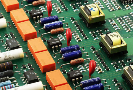
Because the cost of Sn plating is relatively low, Sn plating processing technology is often used for lead-free component welding end and pin surface in production and processing at this stage, but Sn is very easy to produce Sn whiskers. For example, whiskers generated on the pin of PCB components such as interval QFP are very easy to cause short circuit fault, which makes the reliability of electrical equipment have potential safety hazards. The opportunities for the growth of lead-free commercial tin whiskers and the probability of causing adverse effects are far higher than those of lead-free commercial tin whiskers, which will endanger the long-term reliability of electronic equipment.


抖音二維碼

Q Q二維碼

微信二維碼
點(diǎn)擊
然后
聯(lián)系
然后
聯(lián)系
電話熱線
13410863085Q Q

微信

- 郵箱