鑫景福致力于滿足“快速服務,零缺陷,輔助研發”PCBA訂購單需求。


行業新聞

PCB wiring engineer design experience 7
1. Preliminary preparation
This includes preparing component libraries and schematICs. "If you want to do a good job, you must sharpen your tools first "To make a good board, you must draw well in addition to the design principles. When designing PCB boards, first prepare the component library and PCB board of the schematic SCH. The component library can use the library provided by protel, but it is usually difficult to find a suitable one. It is better to make the component library by yourself according to the standard size data of the selected equipment. In principle, make the component library PCB board the first, and then create the component library of SCH. The component library of PCB boards requires high requirements, which directly affects Installation of soundboard; The component library of SCH is relatively loose, as long as you pay attention to the definition of pin content and PCB board components PS: Pay attention to the hidden pins in the standard library After that is the schematIC design. After that, it is ready to start PCB design
2. PCB structure design
In this step, according to the determined PCB size and various mechanical positioning, draw the PCB design environment on the PCB surface, and place the required connectors, buttons/switches, screw holes, assembly holes, etc According to the positioning requirements And fully consider and determine the wiring area and non-wiring area (such as how much area around the screw hole belongs to the non-wiring area).
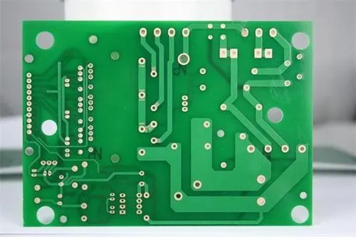
PCB layout
 The layout put it bluntly is to put the device on the board. At this time, if you complete the above preparations:, you can generate a netlist (Design Create Netlist) on the schematic diagram, and then import the netlist (Design Load Nets) on the PCB diagram I saw that the equipment was stacked, and there were flying wires between pins, indicating connection The equipment can then be placed The general layout is carried out according to the following principles:
1) According to the rational division of electrical performance, it is generally divided into: digital circuit area (namely, aircraft of interference and interference), analog circuit area (aircraft of interference), and power drive area (interference source);
2) The circuit that completes the same function should be placed as close as possible, and components should be adjusted to ensure SIMple connection; At the same time, the relative position of each functional block should be adjusted to make the connection between the functional blocks simple;
3) For components with large mass, the installation location and strength shall be considered; The heating elements shall be placed separately from the temperature sensitive parts, and thermal transmission measures should be considered if necessary;
4.) The I/O drive device should be as close as possible to the edge of the printed board and the lead-out connector;
5) The clock generator (such as crystal oscillator or clock oscillator) should be as close as possible to the device that uses the clock;
6) A decoupling capacitor (usually a monolithic capacitor with good high-frequency performance) needs to be added between the power input pin of each integrated circuit and the ground; When the circuit board space is deny, it can also be placed around several integrated circuits to add a tantalum capacitor
7) A discharge diode should be added to the relay coil (1N4148);
8) The layout requirements should be balanced The actual size of the components (captured area and height) and the relative position between components must be considered Ensure the power efficiency of the circuit board and the feasibility and convenience of production and installation. On the prEMIse of reflecting the above principles, properly modify the location of the equipment to make it clean and beautiful For example, the same equipment should be placed neatly and oriented Consistent, not "patched" This step is related to the overall image of the circuit board and the difficulty of wiring in the next step During layout, you can conduct preliminary wiring for uncertain places and take them into full consideration
4. Wiring
Wiring is an important process in the entire PCB design This will directly affect the PCB board In the design process of PCB board, the wiring is generally divided into three parts: the first part is the wiring layout, and the basic requirements are what pcb board design is If the line is not arranged and there are flying lines everywhere, it will be an unqualified board of directors. It can be said that it has not started yet The second is satisfaction with power efficiency This is the quota to measure whether the printed circuit board is qualified This is after routing, carefully adjust the wiring to achieve the best power efficiency Next is beauty If your wiring is connected, it will not affect the efficiency of the electrical appliance. But at first glance, it looks very MESsy and colorful. No matter how good your power efficiency is, it is still a piece of garbage in the eyes of others This brings great inconvenience to testing and maintenance Wiring should be neat and consistent, not without any regular crossing All these must be achieved under the conditions of ensuring electrical efficiency and meeting other personal requirements, otherwise, it will be abandoned The wiring is mainly carried out according to the following principles:
1) In general, the power line and ground wire should be connected first to ensure the power efficiency of the circuit board Within the allowable range, try to widen the width of the power line and ground wire. Preferably, the ground wire is: ground wire>power wire>signal wire, and their relationship is: ground wire>power wire>signal wire. Generally, the width of the signal wire is 0.2-0.3mm, the thinness can reach 0.05-0.07mm, and the power line is 1.2-2.5mm That is, a ground network can be used (the ground of the analog circuit cannot be used in this way)
2) Wire the lines with strict requirements (such as high frequency lines) in advance If necessary, additional grounding wires shall be added for isolation. The wiring of two adjacent layers shall be perpendicular to each other, and parasitic coupling will easily occur in parallel
3) The oscillator shell is grounded. The clock line should be as short as possible and should not be drawn everywhere Under the clock oscillation circuit, the special high-speed logic circuit should not be used to make the surrounding electric field approach zero;
4) Use 45-degree folded lines as much as possible, and do not use 90-degree folded lines to reduce the radiation of high-frequency signals; (double arcs should also be used for lines with high requirements)
5) Do not form a loop in any signal line. The loop should be as SMAll as possible; the vias of the signal line should be as few as possible;
6) The key lines should be as short and thick as possible
7) When transmitting sensitive signals and noise field signals through flat cables
8) Test points should be reserved for key signals to facilitate production and maintenance testing
9) After the schematic wiring is completed; At the same time, after the initial network check and DRC check are correct, the paying off area is filLED with grounding wires, and a large area of copper layer is used for grounding wires The unused parts shall be grounded as grounding wires Or make multilayer PCB board, one layer for power supply and one layer for grounding wire


抖音二維碼

Q Q二維碼

微信二維碼
點擊
然后
聯系
然后
聯系
電話熱線
13410863085Q Q

微信

- 郵箱