鑫景福致力于滿足“快速服務,零缺陷,輔助研發”PCBA訂購單需求。


行業新聞
PCB manufacturer: Introduction to the PCB process that must be used in Protel
Many beginners find Protel software SIMple and easy to learn, but it is diffICult to understand some concepts and terms other than software. In order to promote this powerful EDA tool, the user manual of the software has been published in China. Unfortunately, these books are often written for the software use method itself, and there are few explanations for the concepts in PCB I art that are confusing to readers. The author draws up the items related to PCB technology. Pick some and explain them slightly, so that people can better understand and use this software. If you want to design a qualified printed circuit board diagram, you must first understand the general process flow of modern printed circuit boards, otherwise it will be done behind closed doors.
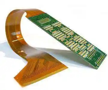
Generally speaking, printed boards are divided into single-sided, double-sided and multilayer boards. The process of single-sided printing plate is relatively simple, which is usually blanking - screen leakage - corrosion - printing material removal - hole processing - MARKing - flux coating - finished product. The process of multi-layer printing plate is relatively complex, that is: inner layer material treatment - positioning hole processing - surface cleaning treatment - making inner layer wiring and graphics - corrosion - pre lamination treatment - outer and inner layer material lamination - hole processing - hole metallization - making outer layer graphics - plating corrosion-resistant weldable metal - removing photoresist - corrosion - plug gold plating - contour processing - hot melting - coating flux - finished product. The process complexity of double-sided board is between the two, so it will not be repeated here.
1. The concept of "Layer"
Similar to the concept of "layer" introduced in word processing or many other software to realize the nesting and composition of drawings, texts, colors, etc., Protel's "layer" is not virtual, but the actual copper foil layers of the printed board material itself. Nowadays, due to the intensive installation of electronic circuit components in SMT processing. For special requirements such as anti-interference and wiring, the printed boards used in some newer electronic products not only have upper and lower sides for wiring, but also have sandwich copper foil that can be specially processed in the middle of the board. For example, the printed board materials used in today's computer motherboards are more than four layers. Because it is relatively difficult to process these layers, most of them are used to set power wiring layers with simple routing (such as Ground Developer and Power Developer in the software), and they are usually wired by means of large area filling (such as ExternaI P1a11e and Fill in the software). The places where the upper and lower surface layers need to be connected with the middle layers are communicated by the so-calLED "Via" mentioned in the software. With the above explanation, it is not difficult to understand the concepts of "multi-layer pad" and "wiring layer setup". To take a simple example, many people have completed wiring and found that many connected terminals do not have pads until printing. In fact, this is because they ignored the concept of "layer" when adding device libraries and did not define the characteristics of their own painted and encapsulated pads as "Mulii Layer". It should be rEMInded that once you have selected the number of layers of the printing plate to be used, you must close those unused layers to avoid causing trouble and detours.
2. Via
In order to connect the lines between layers, a common hole is drilled at the junction of the wires to be connected on each layer, which is called a through hole. Technically, the cylindrical surface of the hole wall of the via is plated with a layer of metal by chemical deposition to connect the copper foil that needs to be connected in the middle layers. The upper and lower sides of the via are made into a common pad shape, which can be directly connected with the lines on the upper and lower sides or not. In general, the following principles shall be followed for the treatment of vias when designing lines:
(1) Minimize the use of vias. Once vias are selected, be sure to handle the gap between them and the surrounding entities, especially the gap between the lines and vias that are not connected between the middle layers and vias that are easy to be ignored. If it is automatic routing, select "on" in the "Via Minimization" submenu to automatically solve the problem.
(2) The larger the current carrying capacity is required, the larger the size of the vias required. For example, the vias used to connect the power layer and stratum with other layers will be larger.
3. Overlay
In order to facilitate the installation and maintenance of the circuit, the required logo patterns and text codes are printed on the upper and lower surfaces of the printed board, such as component label and nominal value, component outline shape and manufacturer's logo, production date, etc. Many beginners only pay attention to the neat and beautiful placement of text symbols when designing the relevant content of the screen layer, ignoring the actual PCB effect. On the printing plate designed by them, characters are either blocked by components or intruded into the soldering area and are wiped on credit. In addition, component labels are printed on adjacent components. Such designs will bring great inconvenience to assembly and maintenance. The correct character layout principle of the silk screen layer is: "no ambiguity, every stitch, beautiful and generous".
4. The particularity of SMD
There are a large number of smd packages in Protel packaging library, that is, surface welded devices. In addition to SMAll size, the biggest feature of this kind of device is the single-sided distributed element pin holes. Therefore, when selecting such devices, the plane where the device is located should be defined to avoid "Missing Plns". In addition, relevant text dimensions of such components can only be placed along the component face.
5. External Plane and Fill
As the name of both, the network shaped filling area is to process a large area of copper foil into a network, and the filling area is only to retain the copper foil completely. In the process of beginner design, there is often no difference between the two on the computer. In fact, as long as you enlarge the drawing, it will be clear at a glance. Just because it is not easy to see the difference between the two, we do not pay attention to the difference between them when using. It should be emphasized that the former has a strong role in suppressing high-frequency interference in circuit characteristics, and is suitable for places that need to be filled in a large area, especially when some areas are used as shielding areas, partition areas or power lines with large current. The latter is mostly used for general line ends or turning areas where small areas need to be filled.
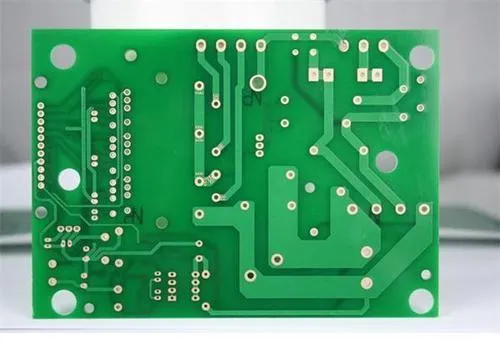
6. Pad
Pad is the most frequently contacted and important concept in PCB design, but beginners tend to ignore its selection and modification, and use circular pads in the design. When selecting the pad type of a component, factors such as the shape, size, layout, vibration and heating, and force direction of the component shall be comprehensively considered. Protel gives a series of pads of different sizes and shapes in the package library, such as round, square, octagonal, round square, and positioning pads, but sometiMES this is not enough, and you need to edit it yourself. For example, the pads with high heat, force and current can be designed as "teardrop" by themselves. Many manufacturers use this form in the design of the familiar color TV PCB's line output transformer pin pads. In general, in addition to the above, the following principles should be considered when editing pads:
(1) When the length of the shape is inconsistent, the size difference between the line width and the specific side length of the pad shall not be too large;
(2) When wiring between leading angles of components is required, pads with asymmetric length shall be selected to achieve half power in the past;
(3) The size of each component pad hole shall be edited and determined according to the component pin thickness. The principle is that the hole size is 0.2 - 0.4 mm larger than the pin diameter.
7. Mask
These films are not only indispensable in PCB manufacturing process, but also necessary for component welding. According to the position and function of "film", "film" can be divided into two categories: component surface (or welding surface) top or bottom and component surface (or welding surface) top or bottomPaste mask. As the name implies, the soldering film is a film coated on the pad to improve the solderability, that is, the light colored round spots on the green board are slightly larger than the pad. The situation of solder mask is just the opposite. In order to make the made board adapt to wave soldering and other welding forms, it is required that the copper foil on the board at the non bonding pad cannot stick tin. Therefore, a layer of paint shall be applied to all parts outside the bonding pad to prevent tin from coating on these parts. It can be seen that these two membranes are complementary. From this discussion, it is not difficult to determine the settings of items like "solver mask En1argement" in the menu.
8. Flying line, flying line has two meanings:
The rubber band like network connection used for observation during automatic routing is called in through the network table and preliminary layout is made, use "The Show command can see the crossing status of the network connections under the layout, and constantly adjust the position of the components to minimize such crossing, so as to obtain the maximum automatic routing routing rate. This step is very important. It can be said that it takes more time, value! In addition, after the automatic routing is completed, you can also use this function to find out which networks have not been deployed. After finding out which networks have not been deployed, you can use manual compensation, The second meaning of "flying wire" is to connect these networks with wires on the printing plate in the future. It should be confessed that if the circuit board is produced in a large number of automatic lines, the flying wire can be designed as a resistance element with a 0 ohm resistance value and a uniform pad spacing.


抖音二維碼

Q Q二維碼

微信二維碼
點擊
然后
聯系
然后
聯系
電話熱線
13410863085Q Q

微信

- 郵箱